|
|
|||||||||
|
|
|
|
|
|
|
|
|
|
|
This chapter contains information about the following topics:
A Design Exchange Format (DEF) file contains the design-specific information of a circuit and is a representation of the design at any point during the layout process. The DEF file is an ASCII representation using the syntax conventions described in "Typographic and Syntax Conventions".
For standard-cell-based/ASIC flow tools, floorplanning is part of the design flow. You typically use the various floorplanning commands to interactively create a floorplan. This data then becomes part of the physical data output for the design using the ROWS, TRACKS, GCELLGRID, and DIEAREA statements. You also can manually enter this data into DEF to create the floorplan.
It is legal for a DEF file to contain only floorplanning information, such as ROWS. In many cases, the DEF netlist information is in a separate format, such as Verilog, or in a separate DEF file. It is also common to have a DEF file that only contains a COMPONENTS section to pass placement information.
Note the following information about creating DEF files:

|
DEF statements end with a semicolon ( ; ). You must leave a space before the semicolon. |
|
|
You must define all objects before you reference them except for the + ORIGINAL argument in the NETS section. |
! " # $ % & ` ( ) * + , / : ; < = > ? @ [ \ ] ^ _ ` { | } ~
A LEF or DEF property string value is contained inside a pair of quotes, like this "<string>". The <string> value can contain any printable ASCII character as shown above, including space, tab, or new-line characters.
Some characters have reserved meanings unless escaped with \.
|
[ ] |
Default special characters for bus bits inside a net or pin name unless overridden by BUSBITCHARS |
|
Default special character for hierarchy inside a net or component name unless overridden by DIVIDERCHAR |
|
|
Matches any sequence of characters for SPECIALNETS or GROUPS component identifiers. |
|
|
Matches any single character for SPECIALNETS or GROUPS component identifiers. |
|
|
The start and end character of a property string value. It has no special meaning for an identifier. |
|
You can use the backslash (\) as an escape character before each of the special characters shown above. When the backslash precedes a character that has a special meaning in LEF or DEF, the special meaning of the character is ignored.
Here are some examples depicting the use of the escape character (\) in identifiers:
|
|
A DEF file with BUSBITCHARS "[]" and net or pin name: |
|
is the 0th member of bus A |
||
|
|
A DEF file with DIVIDERCHAR "/" and net or component names like: |
|
is a 3-level hierarchical name, where C is inside B and B is inside A |
||
|
|
The " character has no special meaning for an identifier. So an identifier would not need a \ before a ". An identifier like: |
name_with_"_in_it
or even
"_name_starts_with_qoute
is legal without a \.
|
|
An identifier that starts with # would be treated as a comment unless the \ is present like this: |
\#_name_with_hash_for_first_char
Note, the # needs to be preceded by white-space to be treated as a comment char, so it has no special meaning inside an identifier. So an identifier like
name_with_#_in_it
is legal without a \.
|
|
Pattern matching characters * or % inside SPECIALNETS or GROUPS component identifiers can be disabled like this: |
GROUPS 1 ;
- myGroup i1/i2/\* ...
or
SPECIALNETS 1 ;
- VDD ( i1/i2/\* VDD ) ...
These will match the exact name i1/i2/* and not match i1/i2/i3 or other components starting with i1/i2/.
Note, the * and % have no special meaning in other identifiers, so no \ is needed for them.
|
|
A real \ char in an identifier needs to be escaped like this: |
name_with_\\_in_it ....
The first \ escapes the second \, so the real name is just name_with_\_in_it.
Properties may have string type values, placed within double quotes ("). However, if you need to use a double quote as a part of the string value itself, you would need to precede it with the escape character (\) to avoid breaking the property syntax. The escape sequence `\"' is converted to `"' during parsing.
The example below depicts the use of the escape character in a quoted property string:
PROPERTY stringQuotedProp "string with \" quote and single backslash \and double backslash \\" ;
The actual value of the property in the database will be:
string with " quote and single backslash and double backslash\
|
|
The first \ escapes the " so it does not end the property string. |
|
|
The next \ has no effect on the subsequent a character. |
|
|
The first \ in \\ escapes the second \ character. This means that the second \ in \\ is treated as a real \ character, and it does not escape the final " character, which ends the property string. |
Note that the other special characters like [ ] / # * % have no special meaning inside a property string and do not need to be escaped.
In DEF syntax, \ is only used to escape characters that have a special meaning if they are not escaped.
Consider the following LEF/DEF header specification:
|
|

|
LEFDEF/[] is equivalent to LEF or DEF with DIVIDERCHAR "/" and BUSBITCHARS "[]" |
|
|
|
LEFDEF|<> is equivalent to LEF or DEF with DIVIDERCHAR "|" and BUSBITCHARS "<>" |
In the following examples, <> are not special characters for LEFDEF/[] files and [] are not special characters for LEFDEF|<> files. Observe how the header settings (listed above) affect the semantic meaning of the names:
|
|
A<0> with LEFDEF/[] is not equivalent to A<0> with LEFDEF|<> |
|
|
A<0> with LEFDEF/[] is equivalent to A\<0\> with LEFDEF|<> |
|
|
A[0] with LEFDEF/[] is equivalent to A<0> with LEFDEF|<> |
For Verilog and DEF equivalence, consider the following DEF header specification:
|
|
|
DEF/[] is equivalent to DEF with DIVIDERCHAR "/" and BUSBITCHARS "[]" |
|
|
|
DEF|<> is equivalent to DEF with DIVIDERCHAR "|" and BUSBITCHARS "<>" |
In the following examples (showing net names), <> are not special characters for DEF/[] files and [] are not special characters for DEF|<> files:
|
|
A<0> in DEF/[] is equivalent to \A<0> in Verilog |
A<0> in DEF|<> is equivalent to A[0] in Verilog (bit 0 of bus A)
|
|
A[0] in DEF/[] is equivalent to A[0] in Verilog (bit 0 of bus A) |
A[0] in DEF|<> is equivalent to \A[0] in Verilog
|
|
A\<0\> in DEF/[] is equivalent to \A<0> in Verilog |
A\<0\> in DEF|<> is equivalent to \A<0> in Verilog
|
|
A\[0\] in DEF/[] is equivalent to \A[0] in Verilog |
A\[0\] in DEF|<> is equivalent to \A[0] in Verilog *
The following example shows instance path names for Verilog and DEF equivalence:
|
|
A/B in DEF/[] represents instance path A.B (instance A in the top module, with instance B inside the module referenced by instance A) in Verilog. |
|
|
A\/B in DEF/[] represents instance \A/B in Verilog. |
|
|
A\/B/C in DEF/[] represents \A/B .C in Verilog (escaped instance \A/B in the top module, with instance C inside the module referenced by instance \A/B). |
|
|
The net and instance path A\/B/C/D[0] in DEF/[] will represent \A/B .C.D[0] in Verilog (escaped instance \A/B in the top module, with instance C inside the module referenced by instance \A/B, and bus D in that module with bit 0 being specified). |
The DEF escape \ applies only to the next character and prevents the character from having a special meaning.
The Verilog escape \ affects the complete "token" and is terminated by a trailing white space (" ", Tab, Enter, etc.).
Standard DEF files can contain the following statements and sections. You can define the statements and sections in any order; however, data must be defined before it is used. For example, you must specify the UNITS statement before any statements that use values dependent on UNITS values, and VIAS statements must be defined before statements that use via names. If you specify statements and sections in the following order, all data is defined before being used.
The following definitions describe the syntax arguments for the statements and sections that make up a DEF file. The statements and sections are listed in alphabetical order, not in the order they must appear in a DEF file. For the correct order, see Order of DEF Statements.
|
COMPONENT compName |
Specifies a component with which to associate a blockage. Specify with LAYER layerName to create a blockage on layerName associated with a component. Specify with PLACEMENT to create a placement blockage associated with a component. |
|
DESIGNRULEWIDTH effectiveWidth |
|
|
Specifies that the blockage has a width of effectiveWidth for the purposes of spacing calculations. If you specify DESIGNRULEWIDTH, you cannot specify SPACING. As a lot of spacing rules in advanced nodes no longer just rely on wire width, DESIGNRULEWIDTH is not allowed for 20nm and below nodes. |
|
|
Creates a blockage on the specified layer where metal fill shapes cannot be placed. |
|
|
LAYER layerName |
Note: Cut-layer blockages will prevent vias from being placed in that area. |
|
MASK maskNum |
Specifies which mask for double or triple patterning lithography to use for the specified shapes. The maskNum variable must be a positive integer. Most applications support values of only 1, 2, or 3. Shapes without any defined mask have no mask set (are uncolored). - LAYER metal1 + PUSHDOWN + MASK 1 RECT ( -300 -310 ) ( 320 330 ) #rectangle on mask 1 RECT ( -150 -160 ) ( 170 180 ); #rectangle on mask 1 |
|
Specifies the number of blockages in the design specified in the BLOCKAGES section. |
|
|
PARTIAL maxDensity |
Indicates that the initial placement should not use more than maxDensity percentage of the blockage area for standard cells. Later placement of clock tree buffers, or buffers added during timing optimization ignore this blockage. The maxDensity value is calculated as: standard cell area in blockage area/blockage area <= maxDensity This can be used to reduce the density in a locally congested area, and preserve it for buffer insertion. |
|
POLYGON pt pt pt |
Specifies a sequence of at least three points to generate a polygon geometry. The polygon edges must be parallel to the x axis, the y axis, or at a 45-degree angle. Each POLYGON statement defines a polygon generated by connecting each successive point, and then the first and last points. The pt syntax corresponds to a coordinate pair, such as x y. Specify an asterisk (*) to repeat the same value as the previous x or y value from the last point. |
|
Specifies that the blockage was pushed down into the block from the top level of the design. |
|
|
RECT pt pt |
|
|
Creates a blockage on the specified layer where slots cannot be placed. |
|
|
SPACING minSpacing |
Specifies the minimum spacing allowed between this particular blockage and any other shape. The minSpacing value overrides all other normal LAYER-based spacing rules, including wide-wire spacing rules, end-of-line rules, parallel run-length rules, and so on. A blockage with SPACING is not "seen" by any other DRC check, except the simple check for minSpacing to any other routing shape on the same layer. The minSpacing value cannot be larger than the maximum spacing defined in the SPACING or SPACINGTABLE for that layer. Tools may change larger values to the maximum spacing value with a warning. |
Example 4-1 Blockages Statements
|
|
The following BLOCKAGES section defines eight blockages in the following order: two metal2 routing blockages, a pushed down routing blockage, a routing blockage attached to component |i4, a floating placement blockage, a pushed down placement blockage, a placement blockage attached to component |i3, and a fill blockage. |
- LAYER metal1
RECT ( -300 -310 ) ( 320 330 )
RECT ( -150 -160 ) ( 170 180 ) ;
- LAYER metal1 + PUSHDOWN
RECT ( -150 -160 ) ( 170 180 ) ;
- LAYER metal1 + COMPONENT |i4
RECT ( -150 -160 ) ( 170 180 ) ;
- PLACEMENT
RECT ( -150 -160 ) ( 170 180 ) ;
- PLACEMENT + PUSHDOWN
RECT ( -150 -160 ) ( 170 180 ) ;
- PLACEMENT + COMPONENT |i3
RECT ( -150 -160 ) ( 170 180 ) ;
- LAYER metal1 + FILLS
RECT ( -160 -170 ) ( 180 190 ) ;
|
|
The following BLOCKAGES section defines two blockages. One requires minimum spacing of 1000 database units for its rectangle and polygon. The other requires that its rectangle's width be treated as 1000 database units for DRC checking. |
- LAYER metal1
+ SPACING 1000 #RECT and POLYGON require at least 1000 dbu spacing
RECT ( -300 -310 ) ( 320 300 )
POLYGON ( 0 0 ) ( * 100 ) ( 100 * ) ( 200 200 ) ( 200 0 ) ; #Has 45-degree #edge
- LAYER metal1
+ DESIGNRULEWIDTH 1000 #Treat the RECT as 1000 dbu wide for DRC checking
RECT ( -150 -160 ) ( 170 180 ) ;
If one of the bus bit characters appears in a DEF name as a regular character, you must use a backslash (\) before the character to prevent the DEF reader from interpreting the character as a bus bit delimiter.
If you do not specify the BUSBITCHARS statement in your DEF file, the default value is "[]".
Example 4-2 Component Mask Shift
The following example indicates that any given component can shift the mask on layers M3, M2, VIA1, or M1:
COMPONENTMASKSHIFT M3 M2 VIA1 M1 ;
This layer list is used to interpret the + MASKSHIFT shiftLayerMasks value for a specific component as shown in the example given below:
+ MASKSHIFT 1102 #M3 shifted by 1, M2 by 1, VIA1 by 0, M1 by 2
...
For details on components, see the Components section.
Defines design components, their location, and associated attributes.
|
Specifies the component name in the design, which is an instance of modelName, the name of a model defined in the library. A modelName must be specified with each compName. |
|
|
COVER pt orient |
Specifies that the component has a location and is a part of a cover macro. A COVER component cannot be moved by automatic tools or interactive commands. You must specify the component's location and its orientation. |
|
EEQMASTER macroName |
|
|
FIXED pt orient |
|
|
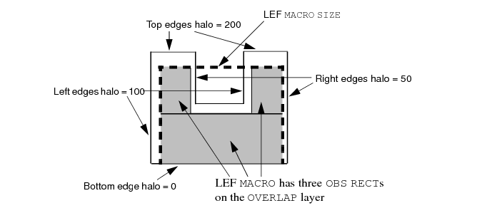
HALO [SOFT] left bottom right top |
|
|
Specifies a placement blockage around the component. The halo extends from the LEF macro's left edge(s) by left, from the bottom edge(s) by bottom, from the right edge(s) by right, and from the top edge(s) by top. The LEF macro edges are either defined by the rectangle formed by the MACRO SIZE statement, or, if OVERLAP obstructions exist (OBS shapes on a layer with TYPE OVERLAP), the polygon formed by merging the OVERLAP shapes. If SOFT is specified, the placement halo is honored only during initial placement; later phases, such as timing optimization or clock tree synthesis, can use the halo area. This can be used to preserve certain areas (such as small channels between blocks) for buffer insertion. |
|
|
MASKSHIFT shiftLayerMasks |
|
|
The shiftLayerMasks variable is a hex-encoded digit, with one digit per multi-mask layer: ...<thirdLayerShift><secondLayerShift><bottomLayerShift> |
|
|
The bottomLayerShift value is the mask-shift for the bottom-most multi-mask layer defined in the COMPONENTMASKSHIFT statement. The secondMaskShift, thirdMaskShift, and so on, are the shift values for each layer in order above the bottom-most multi-mask layer. The missing digits indicate that no shift is needed so 002 and 2 have the same meaning. For 2-mask layers, the LayerShift value must be 0 or 1 and indicates: 1 - Shift the mask colors by 1 (mask 1->2, and 2->1) For 3-mask layers, the LayerShift value can be 0, 1, 2, 3, 4, or 5 that indicates: 1 - Shift by 1 (1->2, 2->3, 3->1) 2 - Shift by 2 (1->3, 2->1, 3->2) 3 - Mask 1 is fixed, swap 2 and 3 4 - Mask 2 is fixed, swap 1 and 3 5 - Mask 3 is fixed, swap 1 and 2 The purpose of 3, 4, 5 is for standard cells that have a fixed power-rail mask color, but the pins between the power-rails can still be shifted. Suppose you had a standard cell with mask 1 power rails, and three signal pins on mask 1, 2, and 3. A LayerShift of 3, will keep the mask 1 power rails and signal pin fixed on mask 1, while mask 2 and mask 3 signal pin shapes will swap mask colors. |
|
Example 4-3 Mask Shift Layers for Components
The following example shows a LEF section that has a three-mask layer defined for M1, and two-mask layer defined for layers VIA1 and M2:
COMPONENTMASKSHIFT M2 VIA1 M1 ;
+ MASKSHIFT 2 #M1 layer masks are shifted by 2, no shift for others
...
+ MASKSHIFT 103 ##M1 layer has shift 3, VIA1 0, M2 1
...
Example 4-4 Component Halo
The following statement creates a placement blockage for a "U-shaped" LEF macro, as illustrated in Figure 4-1 :
- i1/i2
+ PLACED ( 0 0 ) N
+ HALO 100 0 50 200 ;
Figure 4-1 Component Halo
Specifies the number of components defined in the COMPONENTS section.
PLACED pt orient
Specifies that the component has a location, but can be moved using automatic layout tools. You must specify the component's location and orientation.
PROPERTY propName propVal
Specifies a numerical or string value for a component property defined in the PROPERTYDEFINITIONS statement. The propName you specify must match the propName listed in the PROPERTYDEFINITIONS statement.
REGION regionName
Specifies a region in which the component must lie. regionName specifies a region already defined in the REGIONS section. If the region is smaller than the bounding rectangle of the component itself, the DEF reader issues an error message and ignores the argument. If the region does not contain a legal location for the component, the component remains unplaced after the placement step.
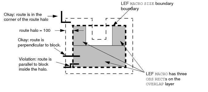
ROUTEHALO haloDist minLayer maxLayer
Specifies that signal routing in the "halo area" around the block boundary should be perpendicular to the block edge in order to reach the block pins. The halo area is the area within haloDist of the block boundary (see the Figure below). A routing-halo is intended to be used to minimize cross coupling between routing at the current level of the design, and routing inside the block. It has no effect on power routing. Note that this also means it is allowed to route in the "halo corners" because routing in the "halo corner" is not adjacent to the block boundary, and will not cause any significant cross-coupling with routing inside the block.
The routing halo exists for the routing layers between minLayer and maxLayer. The layer you specify for minLayer must be a lower routing layer than maxLayer.
Type: Integer, specified in DEF database units (haloDist); string that matches a LEF routing layer name (minLayer and maxLayer)
Example 4-5 Route Halo Example
For a U-shaped macro, the following component description results in the halo shown in Figure 4-2.
- il/i2
+ PLACED ( 0 0 ) N
+ ROUTEHALO 100 metal1 metal3 ;
Figure 4-2 Route Halo
SOURCE {NETLIST | DIST | USER | TIMING}
Specifies the source of the component.
Value: Specify one of the following:
|
Component is generated by the user for some user-defined reason. |
Specifies that the component does not have a location.
WEIGHT weight
Specifies the weight of the component, which determines whether or not automatic placement attempts to keep the component near the specified location. weight is only meaningful when the component is placed. All non-zero weights have the same effect during automatic placement.
Default: 0
|
|
||
|
|
||
|
|
||
|
|
||
|
|
||
|
|
||
|
|
||
|
|
Example 4-6 Die Area Statements
The following statements show various ways to define the die area.
DIEAREA ( 0 0 ) ( 100 100 ) ; #Rectangle from 0,0 to 100,100
DIEAREA ( 0 0 ) ( 0 100 ) ( 100 100 ) ( 100 0 ) ; #Same rectangle as a polygon
DIEAREA ( 0 0 ) ( 0 100 ) ( 50 100 ) ( 50 50 ) ( 100 50 ) ( 100 0 ) ; #L-shaped polygon
DIVIDERCHAR "/" ;
If the divider character appears in a DEF name as a regular character, you must use a backslash (\) before the character to prevent the DEF reader from interpreting the character as a hierarchy delimiter.
If you do not specify the DIVIDERCHAR statement in your LEF file, the default value is "/".
Defines the contents of the extension.
"tag"
Identifies the extension block. You must enclose tag in quotes.
Example 4-7 Extension Statement
CREATOR "company name"
DATE "timestamp"
REVISION "revision number"
|
LAYER layerName |
|
|
MASK maskNum |
Specifies which mask for double or triple patterning lithography to use for the given rectangles or polygons. The maskNum variable must be a positive integer. Most applications support values of 1, 2, or 3 only. Shapes without any defined mask have no mask setting (are uncolored). |
|
MASK viaMaskNum |
The viaMaskNum variable is a hex-encoded three digit value of the form: <topMaskNum><cutMaskNum><bottomMaskNum> For example, MASK 113 means that the top metal and cut layer maskNum is 1, and the bottom metal layer maskNum is 3. A value of 0 means the shape on that layer has no mask assignment (is uncolored), so 013 means the top layer is uncolored. If either the first or second digit is missing, they are assumed to be 0, so 013 and 13 mean the same thing. Most applications support maskNums of 0, 1, 2, or 3 for double or triple patterning. The topMaskNum and bottomMaskNum variables specify which mask the corresponding metal shape belongs to. The via-master metal mask values have no effect. For the cut layer, the cutMaskNum defines the mask for the bottom-most, and then the left-most cut. For multi-cut vias, the via-instance cut masks are derived from the via-master cut mask values. The via-master must have a mask defined for all the cut shapes and every via-master cut mask is "shifted" (from 1 to 2, 2 to1 for two mask layers, and from 1 to 2, 2 to 3, and 3 to 1 for three mask layers) so the lower-left cut matches the cutMaskNum value. Similarly, for the metal layer, the topMaskNum/bottomMaskNum would define the mask for the bottom-most, then leftmost metal shape. For multiple disjoint metal shapes, the via-instance metal masks are derived from the via-master metal mask values. The via-master must have a mask defined for all of the metal shapes, and every via-master metal mask is "shifted" (1->2, 2->1 for two mask layers, 1->2, 2->3, 3->1 for three mask layers) so the lower-left cut matches the topMaskNum/bottomMaskNum value. |
|
Specifies the number of LAYER statements in the FILLS statement, not the number of rectangles. |
|
|
Indicates that the FILL shapes require OPC correction during mask generation. |
|
|
POLYGON pt pt pt |
Specifies a sequence of at least three points to generate a polygon geometry. The polygon edges must be parallel to the x axis, the y axis, or at a 45-degree angle. Each POLYGON statement defines a polygon generated by connecting each successive point, and then the first and last points. The pt syntax corresponds to a coordinate pair, such as x y. Specify an asterisk (*) to repeat the same value as the previous x or y value from the last point. |
|
RECT pt pt |
Specifies the lower left and upper right corner coordinates of the fill geometry. |
|
VIA viaName pt |
Places the via named viaName at the specified (x y) location (pt). viaName must be a previously defined via in the DEF VIAS or LEF VIA section. |
Example 4-8 Fills Statements
|
|
The following FILLS statement defines fill geometries for layers metal1 and metal2: |
FILLS 2 ;
- LAYER metal1
RECT ( 1000 2000 ) ( 1500 4000 )
RECT ( 2000 2000 ) ( 2500 4000 )
RECT ( 3000 2000 ) ( 3500 4000 ) ;
- LAYER metal2
RECT ( 1000 2000 ) ( 1500 4000 )
RECT ( 1000 4500 ) ( 1500 6500 )
RECT ( 1000 7000 ) ( 1500 9000 )
RECT ( 1000 9500 ) ( 1500 11500 ) ;
END FILLS
|
|
The following FILLS statement defines two rectangles and one polygon fill geometries: |
FILLS 1 ;
-LAYER metal1
RECT ( 100 200 ) ( 150 400 )
POLYGON ( 100 100 ) ( 200 200 ) ( 300 200 ) ( 300 100 )
RECT ( 300 200 ) ( 350 400 ) ;
END FILLS
|
|
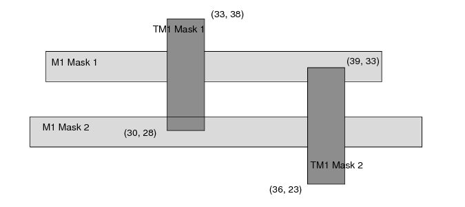
Shapes on the TRIMMETAL layers are written out in the FILLS section in DEF in the following format: |
- LAYER TM1 + MASK x RECT (x x) (x x) ;
The following FILLS statement defines two rectangular shapes on the TRIMMETAL layer TM1, which is defined in a property statement in the masterslice layer section in LEF:
FILLS 2 ;
- LAYER TM1 + MASK 1 RECT (30 28) (33 38)
- LAYER TM1 + MASK 2 RECT (36 23) (39 33)
...
END FILLS
Figure 4-3 Trim Metal Layer Shapes in the FILLS Section
|
|
The following FILLS statement defines two rectangles and two via fill geometries for layer metal1. The rectangles and one of the via fill shapes require OPC correction. |
FILLS 3 ;
-LAYER metal1 + OPC
RECT ( 0 0 ) ( 100 100 )
RECT ( 200 200 ) ( 300 300 ) ;
-VIA via26
( 500 500 )
( 800 800 ) ;
-VIA via28 + OPC
( 900 900 ) ;
END FILLS
Example 4-9 Multi-Mask Patterns for Fills
The following example shows multi-mask patterning for fills:
- LAYER M1 + MASK 1 RECT ( 10 10 ) ( 11 11 ) ; #RECT on MASK 1
- LAYER M2 RECT ( 10 10 ) ( 11 11 ) ; #RECT is uncolored
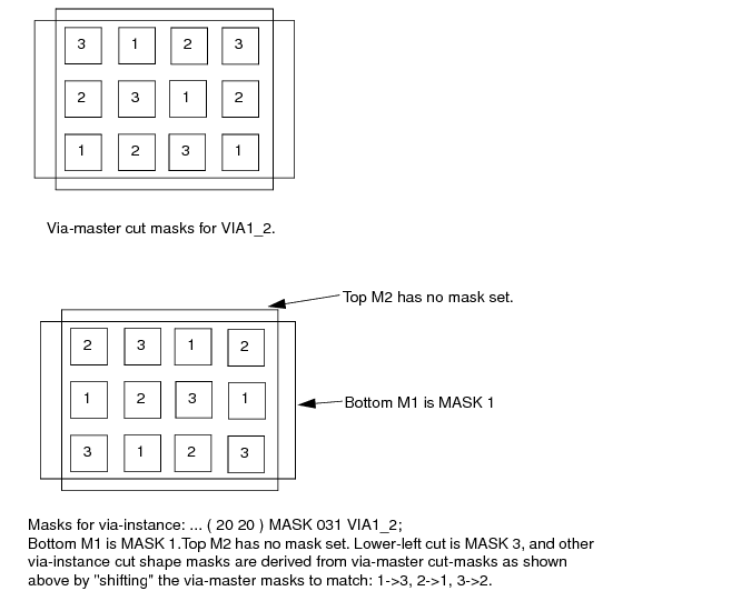
- VIA VIA1_1 + MASK 031 ( 10 10 ) ; #VIA with top-cut-bot mask 031
|
|
M1 rectangle shape is on MASK 1 |
|
|
M2 rectangle shape has no mask set and is uncolored |
|
|
VIA1_1 via will have: |
|
|
|
no mask set for the top metal shape - it is uncolored (topMaskNum is 0 in the 031 value). Note that the via-master color of the top metal shape does not matter. |
|
|
|
mask 1 for the bottom metal shape (bottomMaskNum is 1 in the 031 value) |
|
|
|
for the cut layer, the bottom-most, and then the left-most cut of the via-instance is mask 3. The mask for the other cuts of the via-instance are derived from the via-master by "shifting" the via-master cut masks to match. So if the via-master's bottom- left cut is MASK 1, then the via-master cuts on mask 1 become mask 3 for the via-instance, and similarly cuts on 2 become 1, and cuts on 3 become 2. See Figure 4-11. |
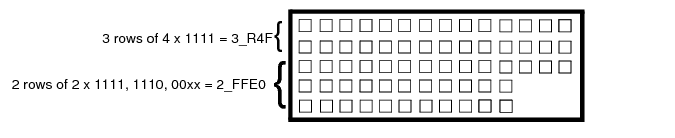
Defines the gcell grid for a standard cell-based design. Each GCELLGRID statement specifies a set of vertical (x) and horizontal (y) lines, or tracks, that define the gcell grid.
Typically, the GCELLGRID is automatically generated by a particular router, and is not manually created by the designer.
DO numColumns+1
Specifies the number of columns in the grid.
DO numRows+1
Specifies the number of rows in the grid.
STEP space
Specifies the spacing between tracks.
X start, Y start
Specify the location of the first vertical (x) and first horizontal (y) track.
For example, the grid formed by the following two GCELLGRID statements creates gcells that are all the same size (100 x 200 in the following):
GCELLGRID X 1000 DO 101 STEP 100 ;
GCELLGRID Y 1000 DO 101 STEP 200 ;
A gcell grid in which all gcells are the same size is called a uniform gcell grid. Adding GCELLGRID statements can increase the granularity of the grid, and can also result in a nonuniform grid, in which gcells have different sizes.
For example, adding the following two statements to the above grid generates a nonuniform grid:
GCELLGRID X 3050 DO 61 STEP 100 ;
GCELLGRID Y 5100 DO 61 STEP 200 ;
Every track segment must belong to a gcell, so gcell grids have the following restrictions:
Gcells grids also have the following restrictions:
|
|
Each GCELLGRID statement must define two lines. |
Specifies the components that make up the group. Do not assign any component to more than one group. You can specify any of the following:
|
|
|
A list of component names separated by spaces, for example, I01 I02 C3204 C3205 |
|
|
|
A pattern for a set of components, for example, IO* and C320* |
Note: An empty group with no component names is allowed.
Specifies the name for a group of components.
Specifies the number of groups defined in the GROUPS section.
PROPERTY propName propVal
Specifies a numerical or string value for a group property defined in the PROPERTYDEFINITIONS statement. The propName you specify must match the propName listed in the PROPERTYDEFINITIONS statement.
REGION regionName
Specifies a rectangular region in which the group must lie. regionName specifies a region previously defined in the REGIONS section. If region restrictions are specified in both COMPONENT and GROUP statements for the same component, the component restriction overrides the group restriction.
Lists a historical record about the design. Each line indicates one record. Any text excluding a semicolon (;) can be included in anyText. The semicolon terminates the HISTORY statement. Linefeed and Return do not terminate the HISTORY statement. Multiple HISTORY lines can appear in a file.
Defines netlist connectivity and regular-routes for nets containing regular pins. These routes are normally created by a signal router that can rip-up and repair the routing. The SPECIALNETS statement defines netlist connectivity and routing for special-routes that are created by "special routers" or "manually" and should not be modified by a signal router. Special routes are normally used for power-routing, fixed clock-mesh routing, high-speed buses, critical analog routes, or flip-chip routing on the top-metal layer to bumps.
Input arguments for a net can appear in the NETS section or the SPECIALNETS section. In case of conflicting values, the DEF reader uses the last value encountered. NETS and SPECIALNETS statements can appear more than once in a DEF file. If a particular net has mixed wiring or pins, specify the special wiring and pins first.
compName pinName
Specifies the name of a regular component pin on a net or a subnet. LEF MUSTJOIN pins, if any, are not included; only the master pin (that is, the one without the MUSTJOIN statement) is included. If a subnet includes regular pins, the regular pins must be included in the parent net.
COVER pt orient
Specifies that the pin has a location and is a part of the cover macro. A COVER pin cannot be moved by automatic tools or by interactive commands. You must specify the pin's location and orientation.
ESTCAP wireCapacitance
Specifies the estimated wire capacitance for the net. ESTCAP can be loaded with simulation data to generate net constraints for timing-driven layout.
FIXED pt orient
Specifies that the pin has a location and cannot be moved by automatic tools, but can be moved by interactive commands. You must specify the pin's location and orientation.
Indicates that the bump net cannot be reassigned to a different pin.
It is legal to have a pin without geometry to indicate a logical connection, and to have a net that connects that pin to two other instance pins that have geometry. Area I/Os have a logical pin that is connected to a bump and an input driver cell. The bump and driver cell have pin geometries (and, therefore, should be routed and extracted), but the logical pin is the external pin name without geometry (typically the Verilog pin name for the chip).
Because bump nets are usually routed with special routing, they also can be specified in the SPECIALNETS statement. If a net name appears in both the NETS and SPECIALNETS statements, the FIXEDBUMP keyword also should appear in both statements. However, the value only exists once within a given application's database for the net name.
Because DEF is often used incrementally, the last value read in is used. Therefore, in a typical DEF file, if the same net appears in both statements, the FIXEDBUMP keyword (or lack of it) in the NETS statement is the value that is used, because the NETS statement is defined after the SPECIALNETS statement.
For an example specifying the FIXEDBUMP keyword, see "Fixed Bump".
FREQUENCY frequency
Specifies the frequency of the net, in hertz. The frequency value is used by the router to choose the correct number of via cuts required for a given net, and by validation tools to verify that the AC current density rules are met. For example, a net described with + FREQUENCY 100 indicates the net has 100 rising and 100 falling transitions in 1 second.
Type: Float
LAYER layerName
Specifies the layer on which the virtual pin lies.
MUSTJOIN (compName pinName)
Specifies that the net is a mustjoin. If a net is designated MUSTJOIN, its name is generated by the system. Only one net should connect to any set of mustjoin pins. Mustjoin pins for macros are defined in LEF. The only reason to specify a MUSTJOIN net in DEF (identified arbitrarily by one of its pins) is to specify prewiring for the MUSTJOIN connection.
Otherwise, nets are generated automatically where needed for mustjoin connections specified in the library. If the input file specifies that a mustjoin pin is connected to a net, the DEF reader connects the set of mustjoin pins to the same net. If the input file does not specify connections to any of the mustjoin pins, the DEF reader creates a local MUSTJOIN net.
Specifies the name for the net. Each statement in the NETS section describes a single net. There are two ways of identifying the net: netName or MUSTJOIN. If the netName is given, a list of pins to connect to the net also can be specified. Each pin is identified by a component name and pin name pair (compName pinName) or as an I/O pin (PIN pinName). Parentheses ensure readability of output. The keyword MUSTJOIN cannot be used as a netName.
NONDEFAULTRULE ruleName
By default the width of any route segment in the NETS regularWiring section is defined by the default width (LEF WIDTH statement value for the routing layer).
This keyword specifies a nondefault rule to use instead of the default rule when creating the net and wiring. When specified with SUBNET, identifies the nondefault rule to use when creating the subnet and its wiring.
The width of any route segment is defined by the corresponding NONDEFAULTRULE WIDTH for that layer.
Wrong-way Width Rules
Some technologies required larger widths for wrong-way routing than in the preferred direction. If the wrong-way width is larger than the default or NDR width, then the wrong-way width is used for wrong-way routes on that layer. The implicit routing extension is still half of the default or NDR width, even for wrong-way routes.
The following LEF DRC rules allow a WRONGDIRECTION keyword that defines wrong-way widths that will affect the width of any wrong-way routes in the DEF NETS section:
LEF58_WIDTH
LEF58_WIDTHTABLE
LEF58_SPANLENGTHTABLE
See the "Impact of Wrong-way Width Rules " section for examples and more details.
Specifies the number of nets defined in the NETS section.
ORIGINAL netName
Specifies the original net partitioned to create multiple nets, including the net being defined.
PATTERN {BALANCED | STEINER | TRUNK | WIREDLOGIC}
Specifies the routing pattern used for the net.
Default: STEINER
Value: Specify one of the following:
|
Used in ECL designs to connect output and mustjoin pins before routing to the remaining pins. |
PIN pinName
Specifies the name of an I/O pin on a net or a subnet.
PLACED pt orient
Specifies that the pin has a location, but can be moved during automatic layout. You must specify the pin's location and orientation.
PROPERTY propName propVal
Specifies a numerical or string value for a net property defined in the PROPERTYDEFINITIONS statement. The propName you specify must match the propName listed in the PROPERTYDEFINITIONS statement.
Specifies the regular physical wiring for the net or subnet. For regular wiring syntax, see "Regular Wiring Statement".
SHIELDNET shieldNetName
Specifies the name of a special net that shields the regular net being defined. A shield net for a regular net is defined earlier in the DEF file in the SPECIALNETS section.
SOURCE {DIST | NETLIST | TEST | TIMING | USER}
Specifies the source of the net. The value of this field is preserved when input to the DEF reader.
Value: Specify one of the following:
SUBNET subnetName
Names and defines a subnet of the regular net netName. A subnet must have at least two pins. The subnet pins can be virtual pins, regular pins, or a combination of virtual and regular pins. A subnet pin cannot be a mustjoin pin.
Used by some tools to indicate that the pin is part of a synthesized scan chain.
USE {ANALOG | CLOCK | GROUND | POWER | RESET | SCAN | SIGNAL | TIEOFF}
Specifies how the net is used.
Value: Specify one of the following:
VPIN vpinName pt pt
Specifies the name of a virtual pin, and its physical geometry. Virtual pins can be used only in subnets. A SUBNET statement refers to virtual pins by the vpinName specified here. You must define each virtual pin in a + VPIN statement before you can list it in a SUBNET statement.
Example 4-10 Virtual Pin
The following example defines a virtual pin:
+ VPIN M7K.v2 LAYER MET2 ( -10 -10 ) ( 10 10 ) FIXED ( 10 10 )
+ SUBNET M7K.2 ( VPIN M7K.v2 ) ( /PREG_CTRL/I$73/A I )
NONDEFAULTRULE rule1
ROUTED MET2 ( 27060 341440 ) ( 26880 * ) ( * 213280 )
M1M2 ( 95040 * ) ( * 217600 ) ( 95280 * )
NEW MET1 ( 1920 124960 ) ( 87840 * )
COVER MET2 ( 27060 341440 ) ( 26880 * )
WEIGHT weight
Specifies the weight of the net. Automatic layout tools attempt to shorten the lengths of nets with high weights. A value of 0 indicates that the net length for that net can be ignored. The default value of 1 specifies that the net should be treated normally. A larger weight specifies that the tool should try harder to minimize the net length of that net.
For normal use, timing constraints are generally a better method to use for controlling net length than net weights. For the best results, you should typically limit the maximum weight to 10, and not add weights to more than 3 percent of the nets.
Default: 1
Type: Integer
XTALK class
Specifies the crosstalk class number for the net. If you specify the default value (0), XTALK will not be written to the DEF file.
Default: 0
Type: Integer
Value: 0 to 200
Specifies regular wiring for the net.
Specifies that the wiring cannot be moved by either automatic layout or interactive commands. If no wiring is specified for a particular net, the net is unrouted. If you specify COVER, you must also specify layerName.
Specifies that the wiring cannot be moved by automatic layout, but can be changed by interactive commands. If no wiring is specified for a particular net, the net is unrouted. If you specify FIXED, you must also specify layerName.
Specifies the layer on which the wire lies. You must specify layerName if you specify COVER, FIXED, ROUTED, or NEW. Specified layers must be routable; reference to a cut layer generates an error.
NEW layerName
Indicates a new wire segment (that is, there is no wire segment between the last specified coordinate and the next coordinate), and specifies the name of the layer on which the new wire lies. Noncontinuous paths can be defined in this manner.
Specifies that the last wide segment of the net is not shielded. If the last segment is not shielded, and is tapered, specify TAPER under the LAYER argument, instead of NOSHIELD.
Specifies that the wiring can be moved by the automatic layout tools. If no wiring is specified for a particular net, the net is unrouted. If you specify ROUTED, you must also specify layerName. An example of DEF NETS routing is shown in DEF NETS Examples.
Defines the center line coordinates of the route on layerName. For information about using routing points, see "Defining Routing Points".
As described above, the width of the routes is defined by the default width (e.g., LEF WIDTH statement on the routing layer) or a NONDEFAULTRULE width for the routing layer. In addition, some technologies require larger widths for wrong-way routes that may increase the width. See the "Impact of Wrong-way Width Rules " section for more details.
The routingPoints syntax is defined as follows:
{ ( x y [extValue] )
{[MASK maskNum] ( x y [extValue] )
|[MASK viaMaskNum] viaName [orient]
|[MASK maskNum] RECT ( deltax1 deltay1 deltax2 deltay2 )
| VIRTUAL ( x y ) } } ...
|
Specifies the amount by which the wire is extended past the endpoint of the segment. The extension value must be greater than or equal to 0 (zero). Some tools only allow 0 or the WIREEXTENSION value from the LAYER or NONDEFAULTRULE statement. |
||
|
MASK maskNum |
||
|
Specifies which mask for double or triple patterning lithography to use for the next wire or RECT. The maskNum variable must be a positive integer - most applications support values of 1, 2, or 3 only. Shapes without any defined mask have no mask set (that is, they are uncolored). |
||
|
MASK viaMaskNum |
||
|
The viaMaskNum variable is a hex-encoded three-digit value of the form: <topMaskNum><cutMaskNum><bottomMaskNum> For example, MASK 113 means that the top metal and cut layer maskNum is 1, and the bottom metal layer maskNum is 3. A value of 0 means that the shape on the layer has no mask assignment (is uncolored), so 013 means the top layer is uncolored. If either the first or second digit is missing, they are assumed to be 0, so 013 and 13 mean the same thing. Most applications support maskNums of 0, 1, 2, or 3 only for double or triple patterning. |
||
|
The topMaskNum and bottomMaskNum variables specify which mask the corresponding metal shape belongs to. The via-master metal mask values have no effect. For the cut layer, the cutMaskNum variable defines the mask for the bottom-most, and then the left-most cut. For multi-cut vias, the via-instance cut masks are derived from the via-master cut mask values. The via-master must have a mask defined for all the cut shapes and every via-master cut mask is "shifted" (from 1 to 2, and 2 to 1 for two mask layers, and from 1 to 2, 2 to 3, and 3 to1 for three mask layers), so the lower-left cut matches the cutMaskNum value. Similarly, for the metal layer, the topMaskNum/bottomMaskNum would define the mask for the bottom-most, then leftmost metal shape. For multiple disjoint metal shapes, the via-instance metal masks are derived from the via-master metal mask values. The via-master must have a mask defined for all of the metal shapes, and every via-master metal mask is "shifted" (1->2, 2->1 for two mask layers, 1->2, 2->3, 3->1 for three mask layers) so the lower-left cut matches the topMaskNum/bottomMaskNum value. |
||
|
Specifies the orientation of the viaName that precedes it, using the standard DEF orientation values of N, S, E, W, FN, FS, FE, and FW (See "Specifying Orientation" ). If you do not specify orient, N (North) is the default non-rotated value used. All other orientation values refer to the flipping or rotation around the via origin (the 0,0 point in the via shapes). The via origin is still placed at the (x y) value given in the routing statement just before the viaName. |
||
|
RECT ( deltax1 deltay1 deltax2 deltay2 ) |
||
|
Indicates that a rectangle is created from the previous ( x y ) routing point using the delta values. The RECT values leave the current point and layer unchanged. |
||
|
Specifies a via to place at the last point. If you specify a via, layerName for the next routing coordinates (if any) is implicitly changed to the other routing layer for the via. For example, if the current layer is metal1, a via12 changes the layer to metal2 for the next routing coordinates. |
||
|
VIRTUAL ( x y ) |
||
|
Indicates that there is a virtual (non-physical zero-width) connection between the previous point and the new ( x y ) point. An '*' indicates that the x or y value is to be used from the previous point. The layer remains unchanged. You can use this keyword to retain the symbolic routing graph. |
||
|
( x y ) |
Specifies the route coordinates. You cannot specify a route with zero length. For more information, see "Specifying Coordinates". |
|
STYLE styleNum
Specifies a previously defined style from the STYLES section in this DEF file. If a style is specified, the wire's shape is defined by the center line coordinates and the style.
Specifies that the next contiguous wire segment on layerName is created using the default rule.
TAPERRULE ruleName
Specifies that the next contiguous wire segment on layerName is created using the specified nondefault rule.
Example 4-11 Multi-mask Patterns for Routing Points
The following example shows a routing statement that specifies three-mask layers M1 and VIA1, and a two-mask layer M2:
+ ROUTED M1 (10 0 ) MASK 3 (10 20 ) VIA1_1
NEW M2 ( 10 10 ) (20 10) MASK 1 ( 20 20 ) MASK 031 VIA1_2 ;
|
|
M1 wire shape (10 0) to (10 20) belongs to mask 3 |
|
|
VIA1_1 via has no preceding MASK statement so all the metal and cut shapes have no mask and are uncolored |
|
|
first NEW M2 wire shape (10 10) to (20 10) has no mask set and is uncolored |
|
|
second M2 wire shape (20 10) to (20 20) is on mask 1 |
|
|
VIA1_2 via has a MASK 031 (it can be MASK 31 also) so: |
|
|
|
topMaskNum is 0 in the 031 value, so no mask is set for the top metal (M2) shape |
|
|
|
bottomMaskNum is 1 in the 031 value, so mask 1 is used for the bottom metal (M1) shape |
|
|
|
cutMaskNum is 3 in the 031 value, so the bottom-most, and then the left-most cut of the via-instance is mask 3. The mask for the other cuts of the via-instance are derived from the via-master by "shifting" the via-master's cut masks to match. So if the via-master's bottom-left cut is mask 1, then the via-master cuts on mask 1 become mask 3 for the via-instance, and similarly cuts on 2 shift to 1, and cuts on 3 shift to 2, as shown in Figure 4-4. |
Figure 4-4 Via-master multi-mask patterns
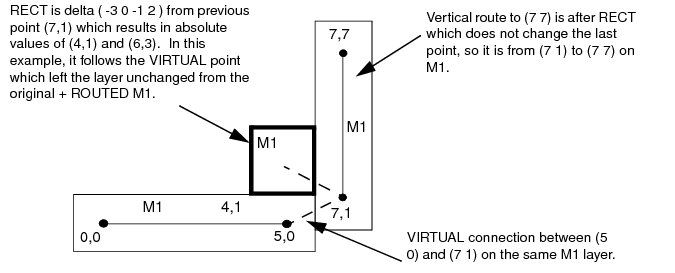
Example 4-12 Routing Points - Usage of Virtual and Rect
Figure 4-5 shows the results of the following routing statement:
+ ROUTED M1 ( 0 0 ) ( 5 0 ) VIRTUAL ( 7 1 ) RECT ( -3 0 -1 2 ) ( 7 7 ) ;
Figure 4-5 Routing Points - Usage of Virtual and Rect
Routing points define the center line coordinates of the route for a specified layer. Routes that are 90 degrees, have a width defined by the routing rule for this wire, and extend from one coordinate (x y) to the next coordinate.
If either endpoint has an extension value (extValue), the wire is extended by that amount past the endpoint. Some applications require the extension value to be 0, half of the wire width, or the same as the routing rule wire extension value. If you do not specify an extension value, the default value of half of the wire width is used.
If the wire segment is a 45-degree edge, and no STYLE is specified, the default octagon style is used for the endpoints. The routing rule width must be an even multiple of the manufacturing grid in order to keep all of the coordinates of the resulting outer wire boundary on the manufacturing grid.
If a STYLE is defined for 90-degree or 45-degree routes, the routing shape is defined by the center line coordinates and the style. No corrections, such as snapping to manufacturing grid, can be applied, and any extension values are ignored. The DEF file should contain values that are already snapped, if appropriate. The routing rule width indicates the desired user width, and represents the minimum allowed width of the wire that results from the style when the 45-degree edges are properly snapped to the manufacturing grid.
To maximize compactness of the design files, the coordinates allow for the asterisk ( * ) convention. Here, ( x * ) indicates that the y coordinate last specified in the wiring specification is used; ( * y ) indicates that the x coordinate last specified is used. Use
( * * extValue ) to specify a wire extension at a via.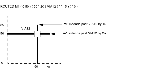
( 100 200 ) ( 200 200 ) ( 200 500 )
The following sequence is an equivalent path:
( 100 200 ) ( 200 * ) ( * 500 )
The following sequence is not valid because it represents a nonorthogonal segment.
( 100 200 ) ( 300 500 )
The following LEF DRC rules allow a WRONGDIRECTION keyword that defines wrong-way widths that will affect the width of any wrong-way routes in the DEF NETS section:
|
Defines the default routing width to use for all regular wiring |
|
|
Defines all the allowable legal widths on the routing layer. |
|
The full syntax for WIDTHTABLE and SPANLENGTHTABLE have an optional ORTHOGONAL keyword or ORTHOGONAL keyword with a value. The ORTHOGONAL keyword and any value after it can be ignored, and has no effect on DEF NETS routing interpretation.
The full syntax for these rules is:
For more information on LEF width rules, see Layer(Routing) section in the "LEF Syntax" chapter in the LEF/DEF Language Reference.
Example 4-13 Impact of default and nondefault rules on wrong-way segment
|
|
This following example shows how LEF width rules will affect the width of any wrong-way routes in the DEF NETS section. An example of each type of rule (WIDTH, WIDTHTABLE, and SPANLENGTHTABLE) is shown below for METAL2: |
LAYER METAL2
...
DIRECTION VERTICAL ;
#0.6 is the default routing rule width in the vertical direction
WIDTH 0.06 ;
#wrong direction (horizontal) metal width must be >= 0.12
PROPERTY LEF58_WIDTH
"WIDTH 0.12 WRONGDIRECTION ; " ;
...
END METAL2
or
LAYER METAL2
...
DIRECTION VERTICAL ;
#0.06 is the default routing rule width in the vertical direction
WIDTH 0.06 ;
#wrong direction (horizontal) metal width must be 0.12, 0.16 or >= 0.20
PROPERTY LEF58_WIDTHTABLE
"WIDTHTABLE 0.06 0.08 0.12 0.16 0.20 ;
WIDTHTABLE 0.12 0.16 0.20 WRONGDIRECTION ; " ;
...
END METAL2
or
LAYER METAL2
...
DIRECTION VERTICAL ;
#0.06 is the default routing rule width in the vertical direction
WIDTH 0.06 ;
#wrong direction (horizontal) metal width must be 0.12, 0.16 or >= 0.20
PROPERTY LEF58_SPANLENGTHTABLE
"SPANLENGTHTABLE 0.06 0.08 0.12 0.16 0.20 ;
SPANLENGTHTABLE 0.12 0.16 0.20 WRONGDIRECTION ; " ;
...
END METAL2
For the above rules, any METAL2 vertical routes are in the preferred direction so they will have the normal widths and extensions as given by the default rule width, or the NONDEFAULTRULE width definition. The horizontal routes are in the wrong-direction, so they will use the first WRONGDIRECTION value in the rules above, that is greater than or equal to the preferred-direction width.
If the rule width is larger than the largest wrong-direction value, then the wrong-direction width is the same as the rule width as shown for NDR7 below.
The table below shows examples of different routing rule widths and the corresponding vertical and horizontal route widths and extensions for the WIDTHTABLE and SPANLENGTHTABLE rules shown above. They both have 0.12, 0.16, and 0.20 as the legal WRONGDIRECTION width values.
For example, the default rule in the table shows that a vertical route in the NETS section will have a width of 0.06 ÎĽm with extension of 0.03 ÎĽm, while a horizontal route will have a wrong-way width of 0.12 ÎĽm with extension 0.03 ÎĽm, as shown in the DEF NETS routing example below:
- NET1 (...)
+ ROUTED METAL2 ( 1 0 ) ( 1 2 ) ( 3 2 ) ( 3 4 ) ;
Figure 4-6 Default rule on wrong way segment
|
|
NDR1 has a width of 0.08 ÎĽm, so it will use the wrong-way width of 0.12, because 0.8 is less than or equal to 0.12 (the first wrong-direction width value). So a vertical route will have a width of 0.08 ÎĽm with extension of 0.04 ÎĽm on a vertical route, while a horizontal route will have a width of 0.12 ÎĽm with extension 0.04 ÎĽm: |
- NET2 (...)
+ NONDEFAULTRULE NDR1
+ ROUTED METAL2 ( 1 0 ) ( 1 3 ) ( 4 3 ) ( 4 5 ) ;
Figure 4-7 Non-Default rule on wrong way segment

|
|
NDR4 in the table has a width of 0.16 ÎĽm. Width of 0.16 is larger than the first wrongdirection value of 0.12, but is less than or equal to the second wrong-direction value of 0.16, so it will use the wrong-way width of 0.16. In this case both the vertical and horizontal routes will have a width of 0.16 ÎĽm with extension of 0.08 ÎĽm. |
- NET3 (...)
+ NONDEFAULTRULE NDR4
+ ROUTED METAL2 (1 0) (1 3) (4 3) (4 4) ;
Figure 4-8 Non-Default rule on wrong way segment
|
|
||
|
|
||
|
|
||
|
|
||
|
|
||
|
|
||
|
|
||
|
|
Example 4-14 Shielded Net
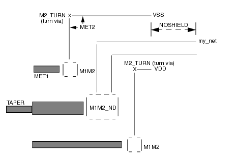
The following example defines a shielded net:
- my_net ( I1 CLK ) ( BUF OUT )
+ SHIELDNET VSS
+ SHIELDNET VDD
ROUTED
MET2 ( 14000 341440 ) ( 9600 * ) ( * 282400 )
M1M2 ( 2400 * )
+ NOSHIELD MET2 ( 14100 341440 ) ( 14000 * )
+ TAPER MET1 ( 2400 282400 ) ( 240 * )
Defines any nondefault rules used in this design that are not specified in the LEF file. This section can also contain the default rule and LEF nondefault rule definitions for reference. These nondefault rule names can be used anywhere in the DEF NETS section that requires a nondefault rule name.
All vias must be previously defined in the LEF VIA or DEF VIAS sections. Every nondefault rule must specify a width for every layer. If a nondefault rule does not specify a via or via rule for a particular routing-cut-routing layer combination, then there must be a VIARULE GENERATE DEFAULT rule that it inherited for that combination.
DIAGWIDTH diagWidth
Specifies the diagonal width for layerName, when 45-degree routing is used.
Default: 0 (no diagonal routing allowed)
Type: Integer, specified in DEF database units
Specifies that any spacing values that exceed the LEF LAYER ROUTING spacing requirements are "hard" rules instead of "soft" rules. By default, routers treat extra spacing requirements as soft rules that are high cost to violate, but not real spacing violations. However, in certain situations, the extra spacing should be treated as a hard, or real, spacing violation, such as when the route will be modified with a post-process that replaces some of the extra space with metal.
LAYER layerName
Specifies the layer for the various width and spacing values. layerName must be a routing layer. Each routing layer must have at least a minimum width specified.
MINCUTS cutLayerName numCuts
Specifies the minimum number of cuts allowed for any via using the specified cut layer. All vias (generated or fixed vias) used for this nondefault rule must have at least numCuts cuts in the via.
Type: (numCuts) Positive integer
Specifies the number of nondefault rules defined in the NONDEFAULTRULES section.
PROPERTY propName propValue
Specifies a property for this nondefault rule. The propName must be defined as a NONDEFAULTRULE property in the PROPERTYDEFINITIONS section, and the propValue must match the type for propName (that is, integer, real, or string).
Specifies the name for this nondefault rule. This name can be used in the NETS section wherever a nondefault rule name is allowed. The reserved name DEFAULT can be used to indicate the default routing rule used in the NETS section.
SPACING minSpacing
Specifies the minimum spacing for layerName. The LEF LAYER SPACING or SPACINGTABLE definitions always apply; therefore it is only necessary to add a SPACING value if the desired spacing is larger than the LAYER rules already require.
Type: Integer, specified in DEF database units.
VIA viaName
Specifies a previously defined LEF or DEF via to use with this rule.
VIARULE viaRuleName
Specifies a previously defined LEF VIARULE GENERATE to use with this routing rule. If no via or via rule is specified for a given routing-cut-routing layer combination, then a VIARULE GENERATE DEFAULT via rule must exist for that combination, and it is implicitly inherited.
WIDTH minWidth
Specifies the required minimum width allowed for layerName.
Type: Integer, specified in DEF database units
WIREEXT wireExt
Specifies the distance by which wires are extended at vias. Enter 0 (zero) to specify no extension. Values other than 0 must be greater than or equal to half of the routing width for the layer, as defined in the nondefault rule.
Default: Wires are extended half of the routing width
Type: Float, specified in microns
Example 4-15 Nondefault Rules
The following NONDEFAULTRULES statement is based on the assumption that there are VIARULE GENERATE DEFAULT rules for each routing-cut-routing combination, and that the default width is 0.3 ÎĽm.
- doubleSpaceRule #Needs extra space, inherits default via rules
+ LAYER metal1 WIDTH 200 SPACING 1000
+ LAYER metal2 WIDTH 200 SPACING 1000
+ LAYER metal3 WIDTH 200 SPACING 1000 ;
- lowerResistance #Wider wires and double cut vias for lower resistance
#and higher current capacity. No special spacing rules,
#therefore the normal LEF LAYER specified spacing rules
#apply. Inherits the default via rules.
+ LAYER metal1 WIDTH 600 #Metal1 is thinner, therefore a little wider
+ LAYER metal2 WIDTH 500
+ LAYER metal3 WIDTH 500
+ MINCUTS cut12 2 #Requires at least two cuts
+ MINCUTS cut23 2 ;
- myRule #Use default width and spacing, change via rules. The
#default via rules are not inherited.
+ LAYER metal1 WIDTH 200
+ LAYER metal2 WIDTH 200
+ LAYER metal3 WIDTH 200
+ VIARULE myvia12rule
+ VIARULE myvia23rule ;
- myCustomRule #Use new widths, spacing and fixed vias. The default
#via rules are not inherited because vias are defined.
+ LAYER metal1 WIDTH 500 SPACING 1000
+ LAYER metal2 WIDTH 500 SPACING 1000
+ LAYER metal3 WIDTH 500 SPACING 1000
+ VIA myvia12_custom1
+ VIA myvia12_custom2
+ VIA myvia23_custom1
+ VIA myvia23_custom2 ;
When the design is a chip rather than a block, the PINS statement describes logical pins, without placement or physical information.
ANTENNAMODEL {OXIDE1 | OXIDE2 | OXIDE3 | OXIDE4}
Specifies the oxide model for the pin. If you specify an ANTENNAMODEL statement, that value affects all ANTENNAGATEAREA and ANTENNA*CAR statements for the pin that follow it until you specify another ANTENNAMODEL statement. The ANTENNAMODEL statement does not affect ANTENNAPARTIAL*AREA and ANTENNADIFFAREA statements because they refer to the total metal, cut, or diffusion area connected to the pin, and do not vary with each oxide model.
Default: OXIDE1, for a new PIN statement
Because DEF is often used incrementally, if an ANTENNA statement occurs twice for the same oxide model, the last value specified is used.
Usually, you only need to specify a few ANTENNA values; however, for a block with six routing layers, it is possible to have six different ANTENNAPARTIAL*AREA values and six different ANTENNAPINDIFFAREA values per pin. It is also possible to have six different ANTENNAPINGATEAREA and ANTENNAPINMAX*CAR values for each oxide model on each pin.
Example 4-16 Antenna Model Statement
The following example describes the OXIDE1 and OXIDE2 models for pin clock1. Note that the ANTENNAPINPARTIALMETALAREA and ANTENNAPINDIFFAREA values are not affected by the oxide values.
+ ANTENNAPINPARTIALMETALAREA 1000 LAYER m1
+ ANTENNAPINDIFFAREA 500 LAYER m1
+ ANTENNAMODEL OXIDE1 #not required, but good practice
+ ANTENNAMAXAREACAR 300 LAYER m1
+ ANTENNAMODEL OXIDE2 #start of OXIDE2 values
+ ANTENNAMAXAREACAR 100 LAYER m1
ANTENNAPINDIFFAREA value [LAYER layerName]
Specifies the diffusion (diode) area to which the pin is connected on a layer. If you do not specify layerName, the value applies to all layers. This is not necessary for output pins.
Type: Integer
Value: Area specified in (DEF database units)2
For more information on process antenna calculation, see Appendix C, "Calculating and Fixing Process Antenna Violations."
ANTENNAPINGATEAREA value [LAYER layerName]
Specifies the gate area to which the pin is connected on a layer. If you do not specify layerName, the value applies to all layers. This is not necessary for input pins.
Type: Integer
Value: Area specified in (DEF database units)2
For more information on process antenna calculation, see Appendix C, "Calculating and Fixing Process Antenna Violations."
ANTENNAPINMAXAREACAR value LAYER layerName
For hierarchical process antenna effect calculation, specifies the maximum cumulative antenna ratio value, using the metal area at or below the current pin layer, excluding the pin area itself. Use this to calculate the actual cumulative antenna ratio on the pin layer, or the layer above it.
Type: Integer
For more information on process antenna calculation, see Appendix C, "Calculating and Fixing Process Antenna Violations."
ANTENNAPINMAXCUTCAR value LAYER layerName
For hierarchical process antenna effect calculation, specifies the maximum cumulative antenna ratio value, using the cut area at or below the current pin layer, excluding the pin area itself. Use this to calculate the actual cumulative antenna ratio for the cuts above the pin layer.
Type: Integer
For more information on process antenna calculation, see Appendix C, "Calculating and Fixing Process Antenna Violations."
ANTENNAPINMAXSIDEAREACAR value LAYER layerName
For hierarchical process antenna effect calculation, specifies the maximum cumulative antenna ratio value, using the metal side wall area at or below the current pin layer, excluding the pin area itself. Use this to calculate the actual cumulative antenna ratio on the pin layer, or the layer above it.
Type: Integer
For more information on process antenna calculation, see Appendix C, "Calculating and Fixing Process Antenna Violations."
ANTENNAPINPARTIALCUTAREA value [LAYER cutLayerName]
Specifies the partial cut area above the current pin layer and inside the macro cell on a layer. If you do not specify layerName, the value applies to all layers. For hierarchical designs, only the cut layer above the I/O pin layer is needed for partial antenna ratio calculation.
Type: Integer
Value: Area specified in (DEF database units)2
For more information on process antenna calculation, see Appendix C, "Calculating and Fixing Process Antenna Violations."
ANTENNAPINPARTIALMETALAREA value [LAYER layerName]
Specifies the partial metal area connected directly to the I/O pin and the inside of the macro cell on a layer. If you do not specify layerName, the value applies to all layers. For hierarchical designs, only the same metal layer as the I/O pin, or the layer above it, is needed for partial antenna ratio calculation.
Type: Integer
Value: Area specified in (DEF database units)2
For more information on process antenna calculation, see Appendix C, "Calculating and Fixing Process Antenna Violations."
ANTENNAPINPARTIALMETALSIDEAREA value [LAYER layerName]
Specifies the partial metal side wall area connected directly to the I/O pin and the inside of the macro cell on a layer. If you do not specify layerName, the value applies to all layers. For hierarchical designs, only the same metal layer as the I/O pin, or the layer above it, is needed for partial antenna ratio calculation.
Type: Integer
Value: Area specified in (DEF database units)2
For more information on process antenna calculation, see Appendix C, "Calculating and Fixing Process Antenna Violations."
COVER pt orient
Specifies the pin's location, orientation, and that it is a part of the cover macro. A COVER pin cannot be moved by automatic tools or by interactive commands. If you specify a placement status for a pin, you must also include a LAYER statement.
DIRECTION {INPUT | OUTPUT | INOUT | FEEDTHRU}
Specifies the pin type. Most current tools do not usually use this keyword. Typically, pin directions are defined by timing library data, and not from DEF.
Value: Specify one of the following:
|
Pin that can accept signals going either in or out of the cell. |
||
FIXED pt orient
Specifies the pin's location, orientation, and that it's location cannot be moved by automatic tools, but can be moved by interactive commands. If you specify a placement status for a pin, you must also include a LAYER statement.
GROUNDSENSITIVITY groundPinName
Specifies that if this pin is connected to a tie-low connection (such as 1'b0 in Verilog), it should connect to the same net to which groundPinName is connected.
groundPinName must match another pin in this PINS section that has a + USE GROUND attribute. The ground pin definition can follow later in this PINS section; it does not have to be defined before this pin definition. It is a semantic error to put this attribute on an existing ground pin. For an example, see Example 4-18.
Note: GROUNDSENSITIVITY is useful only when there is more than one ground net connected to pins in the PINS section. By default, if there is only one net connected to all + USE GROUND pins, the tie-low connections are already implicitly defined (that is, tie-low connections are connected to the same net as any ground pin).
MASK maskNum
Specifies which mask from double or triple patterning to use for the specified shape. The maskNum variable must be a positive integer - most applications support values of 1, 2, or 3 only. Shapes without any defined mask do not have a mask set (are uncolored).
MASK viaMaskNum
Specifies which mask for double or triple patterning lithography is to be applied to via shapes on each layer.
The viaMaskNum variable is a hex-encoded three digit value of the form:
<topMaskNum><cutMaskNum><bottomMaskNum>
For example, MASK 113 means the top metal and cut layer maskNum is 1, and the bottom metal layer maskNum is 3. A value of 0 indicates that the shape on that layer does not have a mask assignment (is uncolored), so 013 means the top layer is uncolored. If either the first or second digit is missing, they are assumed to be 0, so 013 and 13 mean the same thing. Most applications support maskNums of 0, 1, 2, or 3 for double or triple patterning.
The topMaskNum and bottomMaskNum variables specify which mask the corresponding metal shape belongs to. The via-master metal mask values have no effect.
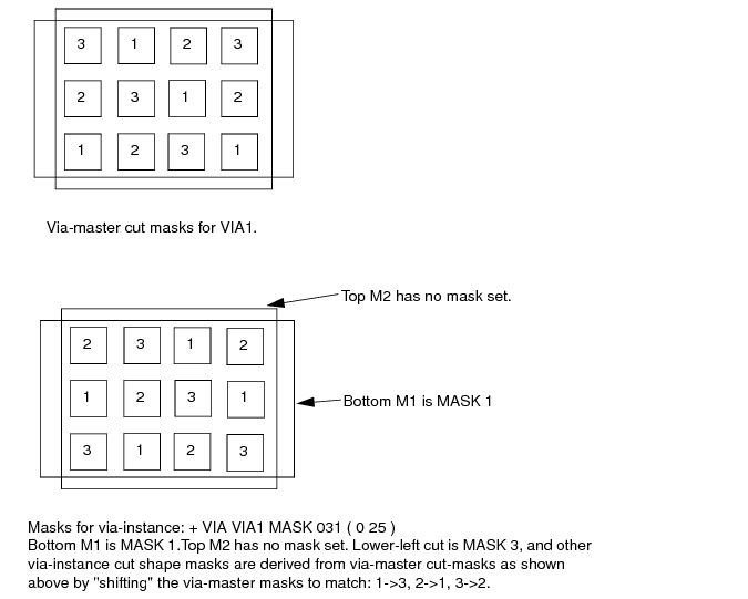
For the cut-layer, the cutMaskNum variable defines the mask for the bottom-most, then the left-most cut in the North (R0) orientation. For multi-cut vias, the via-instance cut masks are derived from the via-master cut mask values. The via-master must have a mask defined for all of the cut shapes and every via-master cut mask is "shifted" (from 1 to 2 and 2 to1 for two mask layers, and from 1 to 2, 2 to 3, and 3 to1 for three mask layers), so the lower-left cut matches the cutMaskNum value. See Example 4-17.
Similarly, for the metal layer, the topMaskNum/bottomMaskNum would define the mask for the bottom-most, then leftmost metal shape. For multiple disjoint metal shapes, the via-instance metal masks are derived from the via-master metal mask values. The via-master must have a mask defined for all of the metal shapes, and every via-master metal mask is "shifted" (1->2, 2->1 for two mask layers, 1->2, 2->3, 3->1 for three mask layers) so the lower-left cut matches the topMaskNum/bottomMaskNum value.
Shapes without any defined mask, that need to be assigned, can be assigned to an arbitrary choice of mask by applications.
Example 4-17 Multi-Mask Patterns for Pins
The following example shows via master masks:
+ LAYER M1 MASK 2 ( -25 0 ) ( 25 50 ) #m1 rectangle is on mask 2
+ LAYER M2 ( -10 0 ) ( 10 75 ) #m2 rectangle, no mask
+ VIA VIA1 MASK 031 ( 0 25 ) #via1 with mask 031
...
The VIA1 via will have:
|
|
no mask set for the top metal shape (topMaskNum is 0 in the 031 value) |
|
|
MASK 1 for the bottom metal shape (botMaskNum is 1 in the 031 value) |
|
|
the bottom-most, and then the left-most cut of the via-instance is MASK 3. The mask for the other cuts of the via-instance are derived from the via-master by "shifting" the via-master cut masks to match. So if the via-master's bottom-left cut is MASK 1, then the via-master cuts on MASK 1 become MASK 3 for the via-instance. Similarly cuts on 2 shift to 1, and cuts on 3 shift to 2. See Figure 4-9. |
Figure 4-9 Multi-Mask Patterns for Pins
NETEXPR "netExprPropName defaultNetName"
Specifies a net expression property name (such as power1 or power2) and a default net name. If netExprPropName matches a net expression property higher up in the netlist (for example, in Verilog, VHDL, or OpenAccess), then the property is evaluated, and the software identifies a net to which to connect this pin. If the property does not exist, defaultNetName is used for the net name.
netExprPropName must be a simple identifier in order to be compatible with other languages, such as Verilog and CDL. Therefore, it can only contain alphanumeric characters, and the first character cannot be a number. For example, power2 is a legal name, but 2power is not. You cannot use characters such as $ and !. The defaultName can be any legal DEF net name.
If more than one pin connects to the same net, only one pin should have a NETEXPR added to it. It is redundant and unnecessary to add NETEXPR to every ground pin connected to one ground net, and it is illegal to have different NETEXPR values for pins connected to the same net.
Example 4-18 Net Expression and Supply Sensitivity
The following PINS statement defines sensitivity and net expression values for five pins in the design myDesign:
- in1 + NET myNet
...
+ SUPPLYSENSITIVITY vddpin1 ; #If in1 is connected to 1'b1, use
#net that is connected to vddpin1.
#No GROUNDSENSITIVITY is needed because
#only one ground net is used by PINS.
#Therefore, 1'b0 implicitly means net
#from any +USE GROUND pin.
- vddpin1 + NET VDD1 + USE POWER
...
+ NETEXPR "power1 VDD1" ; #If an expression named power1 is defined in
#the netlist, use it to fine the net.
#Otherwise, use net VDD1.
- vddpin2 + NET VDD2 + USE POWER
...
+ NETEXPR "power2 VDD2" ; #If an expression named power2 is defined in
#the netlist, use it to find the net.
# Otherise, use net VDD2.
- gndpin1 + NET GND + USE GROUND
...
+ NETEXPR "gnd1 GND" ; #If an expression named gnd1 is defined in
#the netlist, use it to find net
#connection. Otherwise, use net GND.
Specifies the number of pins defined in the PINS section.
pinName + NET netName
Specifies the name for the external pin, and the corresponding internal net (defined in NETS or SPECIALNETS statements).
PLACED pt orient
Specifies the pin's location, orientation, and that it's location is fixed, but can be moved during automatic layout. If you specify a placement status for a pin, you must also include a LAYER statement.
Indicates that the following LAYER, POLYGON, and VIA statements are all part of one PORT connection, until another PORT statement occurs. If this statement is missing, all of the LAYER, POLYGON, and VIA statements are part of a single implicit PORT for the PIN.
This commonly occurs for power and ground pins. All of the shapes of one port (rectangles, polygons, and vias) should already be connected with just the port shapes; therefore, the router only needs to connect to one of the shapes for the port. Separate ports should each be connected by routing inside the block (and each DEF PORT should map to a single LEF PORT in the equivalent LEF abstract for this block).
The syntax for describing PORT statements is defined as follows:
[[+ PORT]
[ + LAYER layerName
[ SPACING minSpacing
| DESIGNRULEWIDTH effectiveWidth]
pt pt
| + POLYGON layerName
[ SPACING minSpacing
| DESIGNRULEWIDTH effectiveWidth]
pt pt pt
| + VIA viaName pt
] ...
]
|
LAYER layerName pt pt |
||
|
Specifies the routing layer used for the pin, and the pin geometry on that layer. If you specify a placement status for a pin, you must include a LAYER statement. |
||
|
POLYGON layerName pt pt pt |
||
|
Each POLYGON statement defines a polygon generated by connecting each successive point, and then the first and last points. The pt syntax corresponds to a coordinate pair, such as x y. Specify an asterisk (*) to repeat the same value as the previous x or y value from the last point. (See Example 4-20.) |
||
|
SPACING minSpacing |
||
|
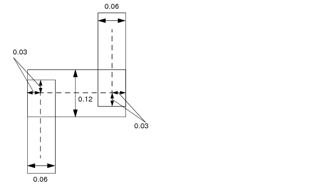
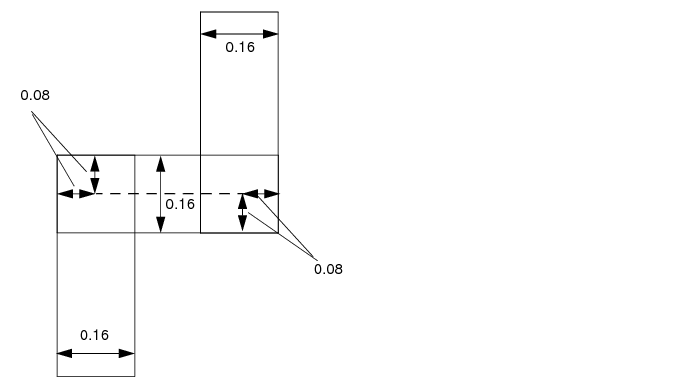
Specifies the minimum spacing allowed between this pin and any other routing shape. This distance must be greater than or equal to minSpacing. If you specify SPACING, you cannot specify DESIGNRULEWIDTH. (See Example 4-21. |
||
|
DESIGNRULEWIDTH effectiveWidth |
||
|
Specifies that this pin has a width of effectiveWidth for the purpose of spacing calculations. If you specify DESIGNRULEWIDTH, you cannot specify SPACING. As a lot of spacing rules in advanced nodes no longer just rely on wire width, DESIGNRULEWIDTH is not allowed for 20nm and below nodes. (See Example 4-21. |
||
|
VIA viaName pt |
||
|
Places the via named viaName at the specified (x y) location (pt). viaName must be a previously defined via in the DEF VIAS or LEF VIA section. |
||
Example 4-19 Port Example
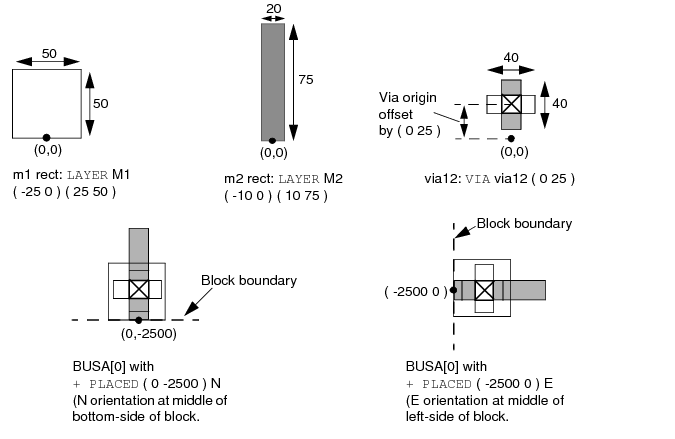
Assume a block that is 5000 x 5000 database units with a 0,0 origin in the middle of the block. If you have the following pins defined, Figure 4-10 illustrates how pin BUSA[0] is created for two different placement locations and orientations:
- BUSA[0] + NEY BUSA[0] + DIRECTION IN{UT + USE SIGNAL
+ LAYER M1 ( -25 0 ) ( 25 50 ) #m1, m2, and via12
+ LAYER M2 ( -10 0 ) ( 10 75 )
+ VIA via12 ( 0 25 )
+ PLACED ( 0 -2500 ) N ; #middle of bottom side
- VDD + NET VDD + DIRECTION INOUT + USE POWER + SPECIAL
+ PORT
+ LAYER M2 ( -25 0 ) ( 25 50 )
+ PLACED ( 0 2500 ) S #middle of top side
+ PORT
+ LAYER M1 (-25 0 ) ( 25 50 )
+ PLACED ( -2500 0 ) E #middle of left side
+ PORT
+ LAYER M1 ( -25 0 ) ( 25 50 )
+ PLACED ( 2500 0 ) W ; #middle of right side
Figure 4-10 Port Illustration
Example 4-20 Port Statement With Polygon
The following PINS statement creates a polygon with a 45-degree angle:
- myPin3 + NET myNet1 + DIRECTION INPUT
+ PORT
+ POLYGON metal1 ( 0 0 ) ( 100 100 ) ( 200 100 ) ( 200 0 ) #45-degree angle
+ FIXED ( 10000 5000 ) N ;
...
Example 4-21 Design Rule Width and Spacing Rules
The following statements create spacing rules using the DESIGNRULEWIDTH and SPACING statements:
- myPin1 + NET myNet1 + DIRECTION INPUT
+ LAYER metal1
DESIGNRULEWIDTH 1000 #Pin is effectively 1000 dbu wide
( -100 0 ) ( 100 200 ) #Pin is 200 x 200 dbu
+ FIXED ( 10000 5000 ) S ;
- myPin2 + NET myNet2 + DIRECTION INPUT
+ LAYER metal1
SPACING 500 #Requires >= 500 dbu spacing
( -100 0 ) ( 100 200 ) #Pin is 200 x 200 dbu
+ COVER ( 10000 5000 ) S ;
- myPin3 + NET myNet1 #Pin with two shapes
+ DIRECTION INPUT
+ LAYER metal2 ( 200 200 ) ( 300 300 ) #100 x 100 dbu shape
+ POLYGON metal1 ( 0 0 ) ( 100 100 ) ( 200 100 ) ( 200 0 ) #Has 45-degree edge
+ FIXED ( 10000 5000 ) N ;
Identifies the pin as a special pin. Regular routers do not route to special pins. The special router routes special wiring to special pins.
SUPPLYSENSITIVITY powerPinName
Specifies that if this pin is connected to a tie-high connection (such as 1'b1 in Verilog), it should connect to the same net to which powerPinName is connected.
powerPinName must match another pin in this PINS section that has a + USE POWER attribute. The power pin definition can follow later in this PINS section; it does not have to be defined before this pin definition. It is a semantic error to put this attribute on an existing power pin. For an example, see Example 4-18.
Note: POWERSENSITIVITY is useful only when there is more than one power net connected to pins in the PINS section. By default, if there is only one net connected to all + USE POWER pins, the tie-high connections are already implicitly defined (that is, tie-high connections are connected to the same net as the single power pin).
USE {ANALOG | CLOCK | GROUND | POWER | RESET | SCAN | SIGNAL | TIEOFF}
Specifies how the pin is used.
Default: SIGNAL
Value: Specify one of the following:
|
Pin is used for connectivity to the chip-level ground distribution network. |
||
|
Pin is used for connectivity to the chip-level power distribution network. |
||
For extra non-bus bit pin names, use the following syntax:
pinname.extraN
N is a positive integer, incremented as the physical pins are added
For example:
PINS n ;
- a + NET a .... ;
- a.extra1 + NET a ... ;
For extra bus bit pin names, use the following syntax:
basename.extraN[index]
basename is simple part of bus bit pin/net name. N is a positive integer, incremented as the physical pins are added. [index] identifies the specific bit of the bus, if it is a bus bit.
For example:
PINS n ;
- a[0] + net a[0] ... ;
- a.extra1[0] + net a[0] ... ;
Note: The brackets [ ] are the BUSBITCHARS as defined in the DEF BUSBITCHARS statement.
|
|
||
|
|
||
|
|
||
|
|
||
|
|
||
|
|
||
|
|
||
|
|
Example 4-22 Pin Statements
The following example describes a physical I/O pin.
# M1 width = 50, track spacing = 120
# M2 width = 60, track spacing = 140
DIEAREA ( -5000 -5000 ) ( 5000 5000 ) ;
TRACKS Y -4900 DO 72 STEP 140 LAYER M2 M1 ;
TRACKS X -4900 DO 84 STEP 120 LAYER M1 M2 ;
# Pin on the left side of the block
- BUSA[0]+ NET BUSA[0] + DIRECTION INPUT
+ LAYER M1 ( -25 0 ) ( 25 165 ) # .5 M1 W + 1 M2 TRACK
+ PLACED ( -5000 2500 ) E ;
# Pin on the right side of the block
- BUSA[1] + NET BUSA[1] + DIRECTION INPUT
+ LAYER M1 ( -25 0 ) ( 25 165 ) # .5 M1 W + 1 M2 TRACK
+ PLACED ( 5000 -2500 ) W ;
# Pin on the bottom side of the block
- BUSB[0] + NET BUSB[0] + DIRECTION INPUT
+ LAYER M2 ( -30 0 ) ( 30 150 ) # .5 M2 W + 1 M1 TRACK
+ PLACED ( -2100 -5000 ) N ;
# Pin on the top side of the block
- BUSB[1] + NET BUSB[1] + DIRECTION INPUT
+ LAYER M2 ( -30 0 ) ( 30 150 ) # .5 M2 W + 1 M1 TRACK
+ PLACED ( 2100 5000 ) S ;
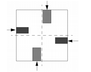
module chip (OUT, BUSA, BUSB) ;
input [0:1] BUSA, BUSB;
output OUT;
The following description for this pin is in the PINS section in the DEF file:
- BUSA[0] + NET BUSA[0] + DIRECTION INPUT ;
- BUSA[1] + NET BUSA[1] + DIRECTION INPUT ;
- BUSB[0] + NET BUSB[0] + DIRECTION INPUT ;
- BUSB[1] + NET BUSB[1] + DIRECTION INPUT ;
- OUT + NET OUT + DIRECTION OUTPUT ;
Defines pin properties in the design.
compName pinName
Specifies a component pin. Component pins are identified by the component name and pin name.
Specifies the number of pins defined in the PINPROPERTIES section.
PIN pinName
Specifies an I/O pin.
PROPERTY propName propVal
Specifies a numerical or string value for a pin property defined in the PROPERTYDEFINITIONS statement. The propName you specify must match the propName listed in the PROPERTYDEFINITIONS statement.
Example 4-23 Pin Properties Statement
- CORE/g76 CKA + PROPERTY CLOCK "FALLING" ;
- comp1 A + PROPERTY CLOCK "EXCLUDED" ;
- rp/regB clk + PROPERTY CLOCK "INSERTION" ;
Lists all properties used in the design. You must define properties in the PROPERTYDEFINITIONS statement before you can refer to them in other sections of the DEF file.
Specifies the object type being defined. You can define properties for the following object types:
Specifies a unique property name for the object type.
Specifies the property type for the object type. You can specify one of the following property types:
RANGE min max
Limits real number and integer property values to a specified range.
value | stringValue
Assigns a numeric value or a name to a DESIGN object.
Note: Assign values to properties for component pins in the PINPROPERTIES section. Assign values to other properties in the section of the LEF file that describes the object to which the property applies.
Specifies the number of regions defined in the design.
PROPERTY propName propVal
Specifies a numerical or string value for a region property defined in the PROPERTYDEFINITIONS statement. The propName you specify must match the propName listed in the PROPERTYDEFINITIONS statement.
Names and defines a region. You define a region as one or more rectangular areas specified by pairs of coordinate points.
Specifies the type of region.
Default: All instances assigned to the region are placed inside the region boundaries, and other cells are also placed inside the region.
Value: Specify one of the following:
Example 4-24 Regions Statement
- REGION1 ( 0 0 ) ( 1200 1200 )
+ PROPERTY REGIONORDER 1 ;
DO numX BY numY
Specifies a repeating set of sites that create the row. You must specify one of the values as 1. If you specify 1 for numY, then the row is horizontal. If you specify 1 for numX, the row is vertical.
Default: Both numX and numY equal 1, creating a single site at this location (that is, a horizontal row with one site).
Specifies the location of the first site in the row.
Type: Integer, specified in DEF database units
PROPERTY propName propVal
Specifies a numerical or string value for a row property defined in the PROPERTYDEFINITIONS statement. The propName you specify must match the propName listed in the PROPERTYDEFINITIONS statement.
Specifies the row name for this row.
Specifies the LEF SITE to use for the row. A site is a placement location that can be used by LEF macros that match the same site. siteName can also refer to a site with a row pattern in its definition, in which case, the row pattern indicates a repeating set of sites that are abutted. For more information, see "Site" and "Macro" in "LEF Syntax."
Specifies the orientation of all sites in the row. siteOrient must be one of N, S, E, W, FN, FS, FE, or FW. For more information on orientations, see "Specifying Orientation".
STEP stepX stepY
Specifies the spacing between sites in horizontal and vertical rows.
Example 4-25 Row Statements
Assume siteA is 200 by 900 database units.
ROW row_0 siteA 1000 1000 N ; #Horizontal row is one-site wide at 1000, 1000
ROW row_1 siteA 1000 1000 N DO 1 BY 1 ; #Same as row_0
ROW row_2 siteA 1000 1000 N DO 1 BY 1 STEP 200 0 ; #Same as row_0
ROW row_3 siteA 1000 1000 N DO 10 BY 1 ; #Horizontal row is 10 sites wide,
#so row width is 200*10=2000 dbu
ROW row_4 siteA 1000 1000 N DO 10 BY 1 STEP 200 0 ; #Same as row_3
ROW row_5 siteA 1000 1000 N DO 1 BY 10 ; #Vertical row is 10 sites high, so
#total row height is 900*10=9000 dbu
ROW row_6 siteA 1000 1000 N DO 1 BY 10 STEP 0 900 ; #Same as row_5
Defines scan chains in the design. Scan chains are a collection of cells that contain both scan-in and scan-out pins. These pins must be defined in the PINS section of the DEF file with + USE SCAN.
Specifies the name of the scan chain. Each statement in the SCANCHAINS section describes a single scan chain.
COMMONSCANPINS [( IN pin )] [( OUT pin )]
Specifies the scan-in and scan-out pins for each component that does not have a scan-in and scan-out pin specified. You must specify either common scan-in and scan-out pins, or individual scan-in and scan-out pins for each component.
FLOATING {floatingComp [( IN pin )] [( OUT pin )] [( BITS numBits )]}
Specifies the floating list. You can have one or zero floating lists. If you specify a floating list, it must contain at least one component.
|
( IN pin ) |
||
|
( OUT pin ) |
||
|
BITS numBits |
Specifies the sequential bit length of any chain element. This allows application tools that do not have library access to determine the sequential bit length contribution of any chain element to ensure the MAXBITS constraints are not violated for chains in a given partition. You can specify 0 to indicate when elements are nonsequential. |
Note: Scan chain reordering commands can use floating components in any order to synthesize a scan chain. Floating components cannot be shared with other scan chains unless they are in the same PARTITION. Each component should only be used once in synthesizing a scan chain.
MAXBITS maxBits
When specified with chains that include the PARTITION keyword, sets the maximum bit length (flip-flop bit count) that the chain can grow to in the partition.
Default: 0 (tool-specific defaults apply, which is probably the number of bits in each chain)
Type: Integer
Value: Specify a value that is at least as large as the size of the current chain.
Specifies the number of scan chains to synthesize.
ORDERED {fixedComp [( IN pin )] [( OUT pin )] [( BITS numBits )]}
Specifies an ordered list. You can specify none or several ordered lists. If you specify an ordered list, you must specify at least two fixed components for each ordered list.
|
( IN pin ) |
||
|
( OUT pin ) |
||
|
BITS numBits |
Specifies the sequential bit length of any chain element. This allows application tools that do not have library access to determine the sequential bit length contribution of any chain element to ensure the MAXBITS constraints are not violated for chains in a given partition. You can specify 0 to indicate when elements are nonsequential. |
Note: Scan chain reordering commands should synthesize these components in the same order that you specify them in the list. Ordered components cannot be shared with other scan chains unless they are in the same PARTITION. Each component should only be used once in synthesizing a scan chain.
PARTITION partitionName
Specifies a partition name. This statement allows reordering tools to determine inter-chain compatibility for element swapping (both FLOATING elements and ORDERED elements). It associates each chain with a partition group, which determines their compatibility for repartitioning by swapping elements between them.
Chains with matching PARTITION names constitute a swap-compatible group. You can change the length of chains included in the same partition (up to the MAXBITS constraint on the chain), but you cannot eliminate chains or add new ones; the number of chains in the partition is always preserved.
If you do not specify the PARTITION keyword, chains are assumed to be in their own single partition, and reordering can be performed only within that chain.
Example 4-26 Partition Scanchain
In the following definition, chain chain1_clock1 is specified without a MAXBITS keyword. The maximum allowed bit length of the chain is assumed to be the sequential length of the longest chain in any clock1 partition.
- chain1_clock1
+ PARTITION clock1
+ START block1/bsr_reg_0 Q
+ FLOATING
block1/pgm_cgm_en_reg_reg ( IN SD ) ( OUT QZ )
...
block1/start_reset_dd_reg ( IN SD ) ( OUT QZ )
+ STOP block1/start_reset_d_reg SD ;
In the following definition, chain chain2_clock2 is specified with a PARTITION statement that associates it with clock2, and a maximum bit length of 1000. The third element statement in the FLOATING list is a scannable register bank that has a sequential bit length of 4. The ORDERED list element statements have total bit lengths of 1 each because the muxes are specified with a maximum bit length of 0.
- chain2_clock2
+ PARTITION clock2
MAXBITS 1000
+ START block1/current_state_reg_0_QZ
+ FLOATING
block1/port2_phy_addr_reg_0_ ( IN SD ) ( OUT QZ )
block1/port2_phy_addr_reg_4_ ( IN SD ) ( OUT QZ )
block1/port3_intfc ( IN SD ) ( OUT MSB ) ( BITS 4 )
...
+ ORDERED
block1/mux1 ( IN A ) ( OUT X ) ( BITS 0 )
block1/ff1 ( IN SD ) ( OUT Q )
+ ORDERED
block1/mux2 ( IN A ) ( OUT X ) ( BITS 0 )
block1/ff2 ( IN SD ) ( OUT Q ) ;
In the following definition, chain chain3_clock2 is also specified with a PARTITION statement that associates it with clock2. This means it is swap-compatible with chain2_clock2. The specified maximum bit length for this chain is 1200.
- chain3_clock2
+ PARTITION clock2
MAXBITS 1200
+ START block1/LV_testpoint_0_Q_reg Q
+ FLOATING
block1/LV_testpoint_0_Q_reg ( IN SE ) ( OUT Q )
block1/tm_state_reg_1_ (IN SD ) ( OUT QZ )
...
In the following definition, chain chain4_clock3 is specified with a PARTITION statement that associates it with clock3. The second element statement in the FLOATING list is a scannable register bank that has a sequential bit length of 8, and default pins. The ORDERED list element statements have total bit lengths of 2 each because the mux is specified with a maximum bit length of 0.
- chain4_clock3
+ PARTITION clock3
+ START block1/prescaler_IO/lfsr_reg1
+ FLOATING
block1/dp1_timers
block1/bus8 ( BITS 8 )
...
+ ORDERED
block1/ds1/ff1 ( IN SD ) ( OUT Q )
block1/ds1/mux1 ( IN B ) ( OUT Y ) ( BITS 0 )
block1/ds1/ff2 ( IN SD ) ( OUT Q )
...
START {fixedInComp | PIN} [outPin]
Specifies the start point of the scan chain. You must specify this point. The starting point can be either a component, fixedInComp, or an I/O pin, PIN. If you do not specify outPin, the router uses the pin specified for common scan pins.
STOP {fixedOutComp | PIN} [inPin]
Specifies the endpoint of the scan chain. You must specify this point. The stop point can be either a component, fixedOutComp, or an I/O pin, PIN. If you do not specify inPin, the router uses the pin specified for common scan pins.
Note the following when defining scan chains.
|
|
For incremental DEF, if you have a COMPONENTS section and a SCANCHAINS section in the same DEF file, the COMPONENTS section must appear before the SCANCHAINS section. If the COMPONENTS section and SCANCHAINS section are in different DEF files, you must read the COMPONENTS section or load the database before reading the SCANCHAINS section. |
Example 4-27 Scan Chain Statements
Nets 100; #Number of nets resulting after scan chain synthesis
- SCAN-1 ( C1 SO + SYNTHESIZED )
( C4 SI + SYNTHESIZED ) + SOURCE TEST ;
- ...
- N1 ( C3 SO + SYNTHESIZED )
( C11 SI + SYNTHESIZED ) ( AND1 A ) ;
- ...
SCANCHAINS 2; #Specified before scan chain ordering
- S1
+ COMMONSCANPINS ( IN SI ) ( OUT SO )
+ START SIPAD OUT
+ FLOATING C1 C2 ( IN D ) ( OUT Q ) C3 C4 C5...CN
+ ORDERED A1 ( OUT Q ) A2 ( IN D ) ( OUT Q ) ...
AM ( N D )
+ ORDERED B1 B2 ... BL
+ STOP SOPAD IN ;
- S2 ... ;
SCANCHAINS 2 ; #Specified after scan chain ordering
- S1
+ START SIPAD OUT
+ FLOATING C1 ( IN SI ) ( OUT SO )
C2 ( IN D ) ( OUT Q )
C3 ( IN SI ( OUT SO ) ... CN ( IN SI ) ( OUT SO )
+ ORDERED A1 ( IN SI ) ( OUT Q )
A2 ( IN D ) ( OUT Q ) ... AM ( IN D ) ( OUT SO )
+ ORDERED B1 ( IN SI ) ( OUT SO )
B2 ( IN SI ) ( OUT SO ) ...
+ STOP SOPAD IN ;
- S2 ... ;
LAYER layerName
Specifies the layer on which to create slots.
Specifies the number of LAYER statements in the SLOTS statement, not the number of rectangles.
POLYGON pt pt pt
Specifies a sequence of at least three points to generate a polygon geometry. The polygon edges must be parallel to the x axis, the y axis, or at a 45-degree angle. Each POLYGON statement defines a polygon generated by connecting each successive point, and then the first and last points. The pt syntax corresponds to a coordinate pair, such as x y. Specify an asterisk (*) to repeat the same value as the previous x or y value from the last point.
Type: DEF database units
RECT pt pt
Specifies the lower left and upper right corner coordinates of the slot geometry.
Example 4-28 Slots Statements
The following statement defines slots for layers MET1 and MET2.
- LAYER MET1
RECT ( 1000 2000 ) ( 1500 4000 )
RECT ( 2000 2000 ) ( 2500 4000 )
RECT ( 3000 2000 ) ( 3500 4000 ) ;
- LAYER MET2
RECT ( 1000 2000 ) ( 1500 4000 )
RECT ( 1000 4500 ) ( 1500 6500 )
RECT ( 1000 7000 ) ( 1500 9000 )
RECT ( 1000 9500 ) ( 1500 11500 ) ;
The following SLOTS statement defines two rectangles and one polygon slot geometries:
- LAYER metal1
RECT ( 100 200 ) ( 150 400 )
POLYGON ( 100 100 ) ( 200 200 ) ( 300 200 ) ( 300 100 )
RECT ( 300 200 ) ( 350 400 ) ;
Input parameters for a net can appear in the NETS section or the SPECIALNETS section. In case of conflicting values for an argument, the DEF reader uses the last value encountered for the argument. NETS and SPECIALNETS statements can appear more than once in a DEF file. If a particular net has mixed wiring or pins, specify the special wiring and pins first.
You can also specify the netlist in the COMPONENTS statement. If the netlist is specified in both NETS and COMPONENTS statements, and if the specifications are not consistent, an error message appears. On output, the writer outputs the netlist in either format, depending on the command arguments of the output command.
Specifies the name of a special pin on the net and its corresponding component. You can use a compNamePattern to specify a set of component names. During evaluation of the pattern match, components that match the pattern but do not have a pin named pinName are ignored. The pattern match character is * (asterisk). For example, a component name of abc/def would be matched by a*, abc/d*, or abc/def.
ESTCAP wireCapacitance
Specifies the estimated wire capacitance for the net. ESTCAP can be loaded with simulation data to generate net constraints for timing-driven layout.
Indicates that the bump net cannot be reassigned to a different pin.
It is legal to have a pin without geometry to indicate a logical connection and to have a net that connects that pin to two other instance pins that have geometry. Area I/Os have a logical pin that is connected to a bump and an input driver cell. The bump and driver cell have pin geometries (and, therefore, should be routed and extracted), but the logical pin is the external pin name without geometry (typically the Verilog pin name for the chip).
Bump nets also can be specified in the NETS statement. If a net name appears in both the NETS and SPECIALNETS statements, the FIXEDBUMP keyword also should appear in both statements. However, the value only exists once within a given application's database for the net name.
Because DEF is often used incrementally, the last value read in is used. Therefore, in a typical DEF file, if the same net appears in both statements, the FIXEDBUMP keyword (or lack of it) in the NETS statement is the value that is used because the NETS statement is defined after the SPECIALNETS statement.
Example 4-29 Fixed Bump
The following example describes a logical pin that is connected to a bump and an input driver cell. The I/O driver cell and bump cells are specified in the COMPONENTS statement. Bump cells are usually placed with + COVER placement status so they cannot be moved manually by mistake.
- driver1 drivercell + PLACED ( 100 100 ) N ;
...
- bumpa1 bumpcell + COVER ( 100 100 ) N ;
- bumpa2 bumpcell + COVER ( 200 100 ) N ;
The pin is assigned in the PIN statement.
- n1 + NET n1 + SPECIAL + DIRECTION INPUT ;
- n2 + NET n2 + SPECIAL + DIRECTION INPUT ;
In the SPECIALNETS statement, the net n1 is assigned to bumpa1 and cannot be reassigned. Note that another net n2 is assigned to bumpa2; however, I/O optimization commands are allowed to reassign bumpa2 to a different net.
- n1 ( driver1 in ) ( bumpa1 bumpin ) + FIXEDBUMP ;
- n2 ( driver2 in ) ( bumpa2 bumpin ) ;
Specifies the name of the net.
ORIGINAL netName
Specifies the original net partitioned to create multiple nets, including the current net.
PATTERN {BALANCED | STEINER | TRUNK | WIREDLOGIC}
Specifies the routing pattern used for the net.
Default: STEINER
Value: Specify one of the following:
|
Used in ECL designs to connect output and mustjoin pins before routing to the remaining pins. |
PIN pinName
Specifies the name of an I/O pin on a net or a subnet.
PROPERTY propName propVal
Specifies a numerical or string value for a net property defined in the PROPERTYDEFINITIONS statement. The propName you specify must match the propName listed in the PROPERTYDEFINITIONS statement.
Specifies the special wiring for the net. For syntax information, see "Special Wiring Statement".
SOURCE {DIST | NETLIST | TIMING | USER}
Specifies how the net is created. The value of this field is preserved when input to the DEF reader.
Used by some tools to indicate that the pin is part of a synthesized scan chain.
USE {ANALOG | CLOCK | GROUND | POWER | RESET | SCAN | SIGNAL | TIEOFF}
Specifies how the net is used.
Value: Specify one of the following:
VOLTAGE volts
Specifies the voltage for the net, as an integer in units of .001 volts. For example, VOLTAGE 1500 in DEF is equal to 1.5 V.
WEIGHT weight
Specifies the weight of the net. Automatic layout tools attempt to shorten the lengths of nets with high weights. Do not specify a net weight larger than 10, or assign weights to more than 3 percent of the nets in a design.
Note: The net constraints method of controlling net length is preferred over using net weights.
Defines the wiring for both routed and shielded nets.
Specifies that the wiring cannot be moved by either automatic layout or interactive commands. If no wiring is specified for a particular net, the net is unrouted. If you specify COVER, you must also specify layerName width.
Specifies that the wiring cannot be moved by automatic layout, but can be changed by interactive commands. If no wiring is specified for a particular net, the net is unrouted. If you specify FIXED, you must also specify layerName width.
Specifies the width for wires on layerName. Normally, only routing layers use this syntax, but it is legal for any layer (cut layer shapes or other layers like masterslice layers normally use the RECT or POLYGON statements). For more information, see "Defining Routing Points".
Vias do not change the route width. When a via is used in special wiring, the previously established routeWidth is used for the next wire in the new layer. To change the routeWidth, a new path must be specified using NEW layerName routeWidth.
Many applications require routeWidth to be an even multiple of the manufacturing grid in order to be fabricated, and to keep the center line on the manufacturing grid.
Type: Integer, specified in database units
NEW layerName routewidth
Indicates a new wire segment (that is, that there is no wire segment between the last specified coordinate and the next coordinate) on layerName, and specifies the width for the wire. Noncontinuous paths can be defined in this manner. For more information, see "Defining Routing Points".
Type: Integer, specified in database units
POLYGON layerName pt pt pt
Specifies a sequence of at least three points to generate a polygon geometry on layerName. The polygon edges must be parallel to the x axis, the y axis, or at a 45-degree angle. Each polygon statement defines a polygon generated by connecting each successive point, then connecting the first and last points. The pt syntax corresponds to a coordinate pair, such as x y. Specify an asterisk (*) to repeat the same value as the previous x or y value from the last point.
Type: (x y) Integer, specified in database units
RECT layerName pt pt
Specifies a rectangle on layer layerName. The two points define opposite corners of the rectangle. The pt syntax corresponds to a coordinate pair, such as x y. You cannot define the same x and y values for both points (that is, a zero-area rectangle is not legal).
Type: (x y) Integer, specified in database units
Specifies that the wiring can be moved by automatic layout tools. If no wiring is specified for a particular net, the net is unrouted. If you specify ROUTED, you must also specify layerName width.
Defines the center line coordinates of the route on layerName. For information on using routing points, see "Defining Routing Points". For an example of special wiring with routing points, see Example 4-31.
The routingPoints syntax is defined as follows:
( x y [extValue])
{ [MASK maskNum] ( x y [extValue])
| [MASK viaMaskNum] viaName [orient]
[DO numX BY numY STEP stepX stepY]
} ...
|
DO numx BY numY STEP stepX stepY |
||
|
Creates an array of power vias of the via specified with viaName. numX and numY specify the number of vias to create, in the x and y directions. Do not specify 0 as a value. stepX and stepY specify the step distance between vias, in the x and y directions, in DEF distance database units. |
||
|
Specifies the amount by which the wire is extended past the endpoint of the segment. |
||
|
MASK maskNum |
||
|
Specifies which mask for double or triple patterning lithography to use for the next wire. The maskNum variable must be a positive integer. Most applications support values of 1, 2, or 3 only. Shapes without any defined mask have no mask set (that is, they are uncolored). |
||
|
MASK viaMaskNum |
||
|
The viaMaskNum variable is a hex-encoded three digit value of the form: <topMaskNum><cutMaskNum><bottomMaskNum> For example, MASK 113 means the top metal and cut layer maskNum is 1, and the bottom metal layer maskNum is 3. A value of 0 means the shape on that layer has no mask assignment (is uncolored), so 013 means the top layer is uncolored. If either the first or second digit is missing, they are assumed to be 0, so 013 and 13 mean the same thing. Most applications support maskNum values of 0, 1, 2, or 3 only for double or triple patterning. |
||
|
The topMaskNum and bottomMaskNum variables specify which mask the corresponding metal shape belongs to. The via-master metal mask values have no effect. For the cut-layer, the cutMaskNum variable will define the mask for the bottom-most, and then the left-most cut. For multi-cut vias, the via-instance cut masks are derived from the via-master cut mask values. The via-master must have a mask defined for all the cut shapes and every via-master cut mask is "shifted" (from 1 to 2, and 2 to 1 for two mask layers, and from 1 to 2, 2 to 3, and 3 to 1 for three mask layers), so the lower-left cut matches the cutMaskNum value. Similarly, for the metal layer, the topMaskNum/bottomMaskNum would define the mask for the bottom-most, then leftmost metal shape. For multiple disjoint metal shapes, the via-instance metal masks are derived from the via-master metal mask values. The via-master must have a mask defined for all of the metal shapes, and every via-master metal mask is "shifted" (1->2, 2->1 for two mask layers, 1->2, 2->3, 3->1 for three mask layers) so the lower-left cut matches the topMaskNum/bottomMaskNum value. |
||
|
Specifies the orientation of the viaName that precedes it, using the standard DEF orientation values of N, S, E, W, FN, FS, FE, and FW (See "Specifying Orientation" ). If you do not specify orient, N (North) is the default non-rotated value used. All other orientation values refer to the flipping or rotation around the via origin (the 0,0 point in the via shapes). The via origin is still placed at the (x y) value given in the routing statement just before the viaName. |
||
|
Specifies a via to place at the last point. If you specify a via, layerName for the next routing coordinates (if any) is implicitly changed to the other routing layer for the via. For example, if the current layer is metal1, a via12 changes the layer to metal2 for the next routing coordinates. |
||
|
( x y ) |
Specifies the route coordinates. You cannot specify a route with zero length. For more information, see "Specifying Coordinates". |
|
Example 4-30 Via Arrays
The following example specifies arrays of via VIAGEN21_2 on metal1 and metal2.
+ ROUTED metal1 150 ( 100 100 ) ( 200 * )
NEW metal1 0 ( 200 100 ) VIAGEN21_2 DO 10 BY 20 STEP 10000 20000
NEW metal2 0 (-900 -30 ) VIAGEN21_2 DO 1000 BY 1 STEP 5000 0
As with any other VIA statement, the DO statement does not change the previous coordinate. Therefore, the following statement creates a metal1 wire of width 50 from ( 200 100 ) to ( 200 200 ) along with the via array that starts at ( 200 100 ).
NEW metal1 50 ( 200 100 ) VIAGEN21_2 DO 10 BY 20 STEP 1000 2000 ( 200 200 )
Example 4-31 Special Wiring With Routing Points
- vdd (*vdd)
+ USE POWER
+ POLYGON metal1 ( 0 0 ) ( 0 100 ) ( 100 100 ) ( 200 200 ) ( 200 0 )
+ POLYGON metal2 ( 100 100 ) ( * 200 ) ( 200 * ) ( 300 300 ) ( 300 100 )
+ RECT metal1 ( 0 0 ) ( 100 200 )
+ ROUTED metal1 100 ( 0 0 50 ) ( 100 0 50 ) via12 ( 100 100 50 )
+ ROUTED metal2 100 + SHAPE RING + STYLE 1 ( 0 0 ) ( 100 100 ) ( 200 100 )
;
Example 4-32 Multi-Mask Layers with Special Wiring
The following example shows a routing statement that specifies three-mask layers M1 and VIA1, and a two-mask layer M2:
+ FIXED + SHAPE RING + MASK 2 + RECT M3 ( 0 0 ) ( 10 10 )
+ ROUTED M1 2000 (10 0 ) MASK 3 (10 20 ) VIA1_1
NEW M2 1000 ( 10 10 ) (20 10) MASK 1 ( 20 20 ) MASK 031 VIA1_2
+ SHAPE STRIPE + VIA VIA3_3 ( 30 30 ) ( 40 40 )
|
|
M3 rectangle shape is on mask 2, has FIXED route status, and shape RING |
|
|
M1 wire shape from (10 0) to (10 20) is on mask 3. |
|
|
VIA1_1 via has no preceding MASK statement so all the metal and cut shapes have no mask and are uncolored |
|
|
first NEW M2 wire shape (10 10) to (20 10) has no mask set and is uncolored |
|
|
second M2 wire shape (20 10) to (20 20) is on mask 1 |
|
|
VIA1_2 via has a MASK 031 (it can be MASK 31 also) so: |
|
|
|
topMaskNum is 0 in the 031 value, so no mask is set for the top metal (M2) shape |
|
|
|
bottomMaskNum is 1 in the 031 value, so mask 1 is used for the bottom metal (M1) shape |
|
|
|
cutMaskNum is 3 in the 031 value, so the bottom-most, then left-most cut of the via-instance is mask 3. The mask for the other cuts of the via-instance are derived from the via-master by "shifting" the via-master's cut masks to match. So, if the via-master's bottom-left cut is mask 1, then the via-master cuts on mask 1 become mask 3 for the via-instance, and similarly cuts on 2 shift to 1, and cuts on 3 shift to 2. See Figure 4-11. |
The VIA3_3 has shape STRIPE, and the via is at both (30 30) and (40 40). There is no wire segment between (30 30) and (40 40). If the route status is not specified, it is considered as + ROUTED.
Figure 4-11 Multi-Mask Patterns with Special Wiring
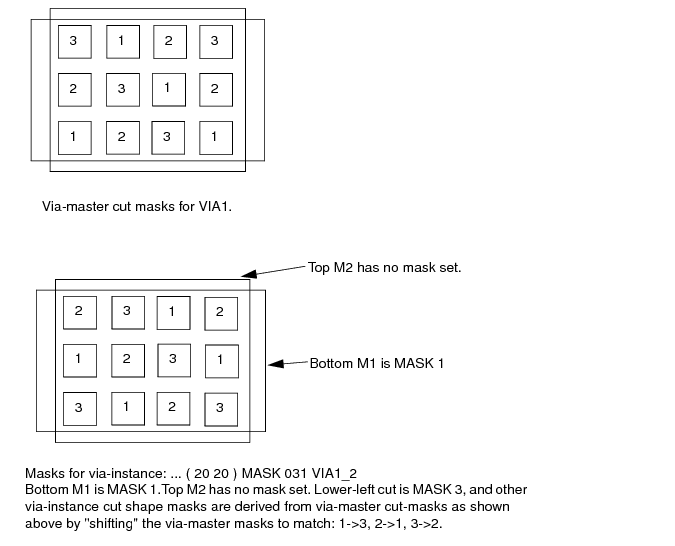
Specifies a wire with special connection requirements because of its shape. This applies to vias as well as wires.
Value: Specify one of the following:
|
Used as a fill shape to correct DRC errors, such as SPACING, MINENCLOSEDAREA, or MINSTEP violations on wires and pins of the same net (see Figure 4-12.) |
Figure 4-12 Fill Shapes
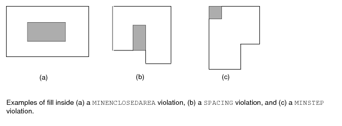
SHIELD shieldNetName
Specifies the name of a regular net to be shielded by the special net being defined.
After describing shielded routing for a net, use + ROUTED to return to the routing of the special net being defined.
STYLE styleNum
Specifies a previously defined style from the STYLES section in this DEF file. The style is used with the endpoints of each routing segment to define the routing shape, and applies to all routing segments defined in one routingPoints statement.
VIA viaName [orient] pt ...
Specifies the name of the via placed at every point in the list with an optional orientation. For example, the statement
VIA myVia ( 0 0 ) ( 1 1 ) indicates an instance of myVia at 0,0 and at 1,1.
...
Example 4-33 Special Nets Statements
Signoff DRC tools may require metal shapes under the trim metal shapes to fill up the gaps between the line-end of wires sandwiched by the trim metal shape to be output in DEF. Those metal shapes would be written out in _TRIMMETAL_FILLS_RESERVED with the DRCFILL tag in the SPECIALNETS section in the following format:
+ ROUTED + SHAPE DRCFILL + MASK x + RECT M1 (x x) (x x)
As trim metal shapes need to be aligned and merged, dummy patches are often added even on OBS and unconnected pins. Those patches would be written out in _SADP_FILLS_RESERVED with the DRCFILL tag in the SPECIALNETS section in the following format:
+ ROUTED + SHAPE DRCFILL + MASK x + RECT M1 (x x) (x x)
The following SPECIALNETS statement defines two metal shapes under the trim metal shapes and a dummy patch written out with the DRCFILL tag:
+ ROUTED + SHAPE DRCFILL + MASK 1 + RECT M1 (30 32) (33 34)
+ ROUTED + SHAPE DRCFILL + MASK 2 + RECT M1 (36 27) (39 29)
+ ROUTED + SHAPE DRCFILL + MASK 2 + RECT M1 (30 27) (36 29)
Figure 4-13 Trim Metal and SADP Fills in the SPECIALNETS Section
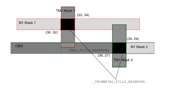
Routing points define the center line coordinates of a route. If a route has a 90-degree edge, it has a width of routeWidth, and extends from one coordinate (x y) to the next coordinate.
If either endpoint has an optional extension value (extValue), the wire is extended by that amount past the endpoint. If a coordinate with an extension value is specified after a via, the wire extension is added to the beginning of the next wire segment after the via (zero-length wires are not allowed). Some applications convert the extension value to an equivalent route that has the x and y points already extended, with no extension value. If no extension value is defined, the wire extension is 0, and the wire is truncated at the endpoint.
The routeWidth must be an even value to ensure that the corners of the route fall on a legal database coordinate without round off. Because most vendors specify a manufacturing grid, routeWidth must be an even multiple of the manufacturing grid in order to be fabricated.
If the wire segment is a 45-degree edge, and no STYLE is specified, the default octagon style is used for the endpoints. The routeWidth must be an even multiple of the manufacturing grid in order to keep all of the coordinates of the resulting outer wire boundary on the manufacturing grid.
If a STYLE is defined for 90-degree or 45-degree routes, the routing shape is defined by the center line coordinates and the style. No corrections, such as snapping to manufacturing grid, should be applied, and any extension values are ignored. The DEF file should contain values that are already snapped, if appropriate. The routeWidth indicates the desired user width, and represents the minimum allowed width of the wire that results from the style when the 45-degree edges are snapped to the manufacturing grid. See Figure 4-15 through Figure 4-24 for examples.
To maximize compactness of the design files, the coordinates allow for the asterisk ( * ) convention. For example, ( x * ) indicates that the y coordinate last specified in the wiring specification is used; ( * y ) indicates that the x coordinate last specified is used.
( 100 200 ) ( 200 200 ) ( 200 500 )
The following sequence is an equivalent path:
( 100 200 ) ( 200 * ) ( * 500 )
The following sequence is not valid because it is not an orthogonal or 45-degree segment.
( 100 200 ) ( 300 500 )
Pins that appear in the SPECIALNETS statement are special pins. Regular routers do not route to these pins. The special router routes special wiring to special pins. If you use a component-based format to input the connectivity for the design, special pins to be routed by the special router also must be specified in the SPECIALNETS statement, because pins included in the COMPONENTS statement are considered regular.
The following example inputs connectivity in a component-based format, specifies VDD and VSS pins as special pins, and marks VDD and VSS nets for special routing:
COMPONENTS 3 ;
C1 AND N1 N2 N3 ;
C2 AND N4 N5 N6 ;
END COMPONENTS
SPECIALNETS 2 ;
VDD ( * VDD ) + WIDTH M1 5 ;
VSS ( * VSS ) ;
END SPECIALNETS
If, in a non-routed design, a net has + SHIELDNET attributes, the router adds shielded routing to this net. + NOSHIELD indicates the last wide segment of the net is not shielded. If the last segment is not shielded and is tapered, use the + TAPER keyword instead of + NOSHIELD. For example:
+ SHIELDNET VSS # both sides will be shielded with VSS
+ SHIELDNET VDD # one side will be shielded with VDD and
+ SHIELDNET VSS # one side will be shielded with VSS
After you add shielded routing to a special net, it has the following syntax:
+ SHIELD regularNetName
MET2 regularWidth ( x y )
A shield net specified for a regular net should be defined earlier in the DEF file in the SPECIALNETS section. After describing shielded routing for a net, use + ROUTED to return to the routing of the current special net.
- VSS
+ ROUTED MET2 200
...
+ SHIELD my_net MET2 100 ( 14100 342440 ) ( 13920 * )
M2_TURN ( * 263200 ) M1M2 ( 2400 * ) ;
- VDD
+ ROUTED MET2 200
...
+ SHIELD my_net MET2 100 ( 14100 340440 ) ( 8160 * )
M2_TURN ( * 301600 ) M1M2 ( 2400 * );
Specifies the number of styles specified in the STYLES section.
STYLE styleNum pt pt
Defines a new style. styleNum is an integer that is greater than or equal to 0 (zero), and is used to reference the style later in the DEF file. When defining multiple styles, the first styleNum must be 0 (zero), and any following styleNum should be numbered consecutively so that a table lookup can be used to find them easily.
Style numbers are keys used locally in the DEF file to reference a particular style, but not actual numbers preserved in the application. Each style number must be unique. Style numbers can only be used inside the same DEF file, and are not preserved for use in other DEF files. Because applications are not required to preserve the style number itself, an application that writes out an equivalent DEF file might use different style numbers.
Type: Integer
The pt syntax specifies a sequence of at least two points to generate a polygon geometry. The syntax corresponds to a coordinate pair, such as x y. Specify an asterisk (*) to repeat the same value as the previous x (or y) value from the last point. The polygon must be convex. The polygon edges must be parallel to the x axis, the y axis, or at a 45-degree angle, and must enclose the point (0 0).
Type: Integer, specified in DEF database units
Example 4-34 Styles Statement
The following STYLES statement defines the basic octagon shown in Figure 4-14.
- STYLE 1 ( 30 10 ) ( 10 30 ) ( -10 30 ) ( -30 10 ) ( -30 -10 )
( -10 -30 ) ( 10 -30 ) ( 30 -10 ) ;
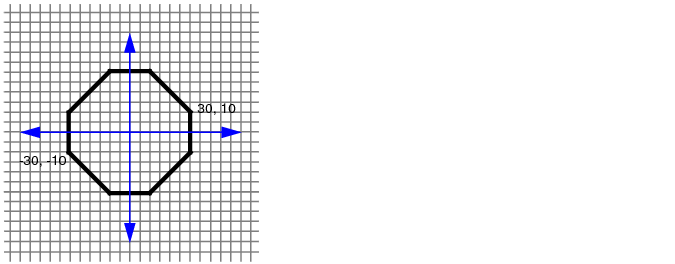
A style is defined as a polygon with points P1 through Pn. The center line is given as (X0, Y0) to (X1, Y1). Two sets of points are built (P0,1 through P0,n and P1,1 through P1,n) as follows:
P0,i = Pi + (X0, Y0) for 1 <= i <= n
P1,i = Pi + (X1, Y1) for 1 <= i <= n
The resulting wire segment shape is a counterclockwise, eight-sided polygon (S1 through S8) that can be computed in the following way:
S1 = lowest point in (left-most points in (P0,1 through P0,n P1,1 through P1,n))
S2 = left-most point in (lowest points in (P0,1 through P0,n P1,1 through P1,n))
S3 = right-most point in (lowest points in (P0,1 through P0,n P1,1 through P1,n))
S4 = lowest point in (right-most points in (P0,1 through P0,n P1,1 through P1,n))
S5 = highest point in (right-most points in (P0,1 through P0,n P1,1 through P1,n))
S6 = right-most point in (highest points in (P0,1 through P0,n P1,1 through P1,n))
S7 = left-most point in (highest points in (P0,1 through P0,n P1,1 through P1,n))
S8 = highest point in (left-most points in (P0,1 through P0,n P1,1 through P1,n))
When consecutive points are collinear, only one of them is relevant, and the resulting shape has less than eight sides, as shown in Figure 4-15. A more advanced algorithm can order the points and only have to check a subset of the points, depending on which endpoint was used, and whether the wire was horizontal, vertical, a 45-degree route, or a 135-degree route.
The following examples illustrate the use of styles for X routing. In two cases, there are examples of SPECIALNETS syntax and NETS syntax that result in the same geometry.
The following statements define an X wire with octagonal ends, as shown in Figure 4-16.
- STYLE 0 ( 30 10 ) ( 10 30 ) ( -10 30 ) ( -30 10 ) ( -30 -10 ) ( -10 -30 )
( 10 -30 ) ( 30 -10 ) ; #An octagon.
- VSS ...
+ ROUTED metal3 50 + STYLE 0 ( 0 0 ) ( 150 150 ) ( 300 0 ) ( 400 0 ) ;
#The style applies to all the segments until a NEW statement or ";"
#at the end of the net.
- mySignal ...
+ ROUTED metal3 STYLE 0 ( 0 0 ) ( 150 150 ) ( 300 0 ) ( 400 0 ) ;
#The style applies to all the segments in the ROUTED statement
The following statements define the same X wire with mixed octagonal and manhattan styles, as shown in Figure 4-17.
- STYLE 0 ( 30 10 ) ( 10 30 ) ( -10 30 ) ( -30 10 ) ( -30 -10 ) ( -10 -30 )
( 10 -30 ) ( 30 -10 ) ; #An octagon
- STYLE 1 ( 25 25 ) ( -25 25 ) ( -25 -25 ) ( 25 -25 ) ; #A square
- POWER (* power)
+ ROUTED metal3 50 + STYLE 0 ( 0 0 ) ( 150 150 )
NEW metal3 50 + STYLE 1 ( 150 150 ) ( 300 0 ) ( 400 0 ) ;
- mySignal ...
+ ROUTED metal3 STYLE 0 ( 0 0 ) ( 150 150 )
NEW metal3 STYLE 1 ( 150 150 ) ( 300 0 ) ( 400 0 ) ;
Note: The square ends might be necessary for connecting to manhattan wires or pins, or in cases where vias have a manhattan shape even on X routing layers. In practice, the middle wire probably would not use a simple square, such as style2; it would use a combination of an octagon and a square for the middle segment style, in order to smooth out the resulting outline at the (150,150) point.
The following statements define a manhattan wire with a width of 70, as shown in Figure 4-18.
This example emphasizes that the style overrides the width of 100 units. In this case, the style polygon is a square 70 x 70 units wide, and the vias (via12) are 100 x 100 units wide. The application that creates the styles is responsible for meeting any particular width requirements. Normally, the resulting style-computed width is equal to or larger than the wire width given in the routing statement.
- STYLE 0 ( 35 35 ) ( -35 35 ) ( -35 -35 ) ( 35 -35 ) ;
- POWER ...
+ ROUTED metal1 100 + STYLE 0 ( 0 0 ) via12 ( 600 * ) via12 ;

The following statements define a similar wire that is offset from the center, as shown in Figure 4-19. Similar to Example 3, the center line in both runs through the middle of the X in the vias.
- STYLE 0 ( 35 20 ) ( -35 20 ) ( -35 -50 ) ( 35 -50 ) ; #70 x 70 offset square
- POWER ...
+ ROUTED metal1 100 + STYLE 0 ( 0 0 ) via12 ( 600 * ) via12 ;

The following statements define a wire that uses a "2-point line" style, as shown in Figure 4-20.
- STYLE 0 ( 0 -10 ) ( 0 10 ) ; #a vertical line
- POWER ...
+ ROUTED metal1 20 + STYLE 0 ( 0 0 ) ( 100 0 ) ;
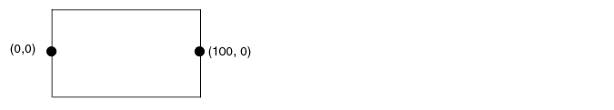
The default style is an octagon (shown in Figure 4-21 ) whose coordinates are computed from the wire width and the manufacturing grid.
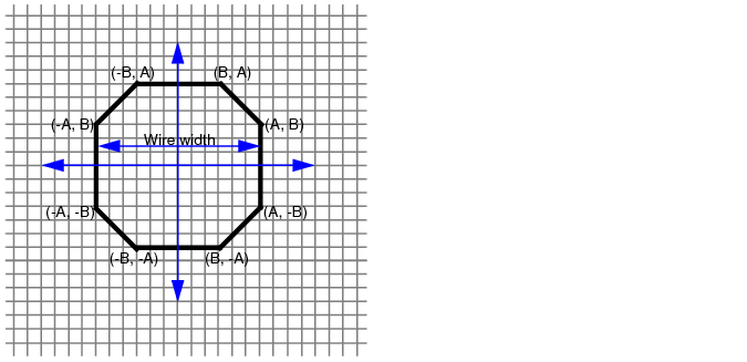
|
|
M = manufacturing grid (mgrid). This is derived from the LEF MANUFACTURINGGRID statement. |
The octagon coordinates are computed as:
A = W/2
B = [ceiling(W/(sqrt(2) * M) ) * M] - A
The derivation of B can be understood as:
D = sqrt( (A + B)2 + (A + B)2) or D = sqrt(2) * (A + B)
D/sqrt(2) = A + B
B = D/sqrt(2) - A or W/sqrt(2) - A
B on mgrid = ceiling(B / M) * M
Which results in the computation:
B = [ceiling(W/(sqrt(2) * M) ) * M] - A
The following table lists examples coordinate computations:
|
W = Width (ÎĽm) |
M = mgrid (ÎĽm) |
A (ÎĽm) |
B (ÎĽm) |
Diagonal width (ÎĽm) |
||
The following two routes produce identical routing shapes, as shown in Figure 4-22.
- POWER (* power)
+ ROUTED metal3 80 ( 0 0 ) ( 100 0 ) ( 200 100 ) ( 300 100 ) ;
- mySignal ... #mySignal uses the default routing rule width of 80
+ ROUTED metal3 ( 0 0 0 ) ( 100 0 0 ) ( 200 100 0 ) ( 300 100 0 ) ;
#The wire extension was set to 0 for every point. The wire extension
#is ignored for 45-degree route segments; the default octagon
#overrides it.
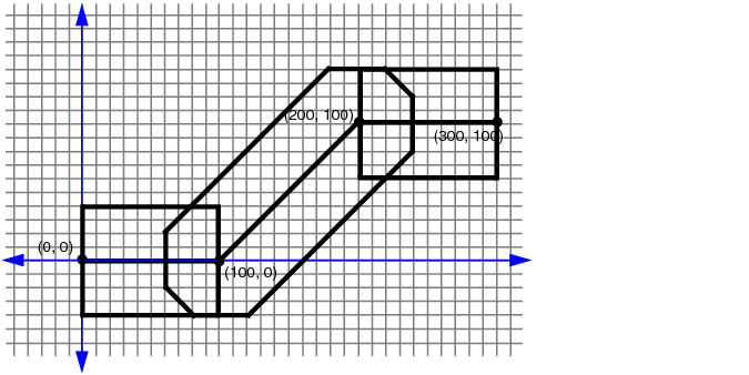
The following regular route definition, using the traditional default wire extension of 1/2 * width for the first and last 90-degree endpoints, produces the route shown in Figure 4-23.
- POWER (* power) #The half-width extensions are given for the first and last
+ ROUTED metal3 80 ( 0 0 40 ) ( 100 0 ) ( 200 100 ) ( 300 100 40 ) ;
#The default extension is 0 for SPECIALNETS, so it is not given for
- mySignal ... #mySignal uses the default routing rule with width of 80
+ ROUTED metal3 ( 0 0 ) ( 100 0 0 ) ( 200 100 0 ) ( 300 100 ) ;
#The default extension is half the width for NETS, so it is not
#included for the first and last end-points.
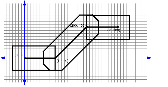
The following definition, using the traditional default wire extension of 1/2 * width for all of the points, produces the route in Figure 4-24.
- POWER (* power) #The half-width extensions are given explicitly
+ ROUTED metal3 80 ( 0 0 40 ) ( 100 40 ) ( 200 100 40 ) ( 300 100 40 ) ;
- mySignal ... #mySignal uses the default routing rule width of 80
+ ROUTED metal3 ( 0 0 ) ( 100 0 ) ( 200 100 ) ( 300 100 ) ;
#All points use the implicit default 1/2 * width wire extensions.
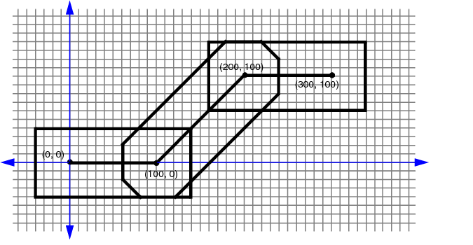
Defines the routing grid for a standard cell-based design. Typically, the routing grid is generated when the floorplan is initialized. The first track is located at an offset from the placement grid set by the OFFSET value for the layer in the LEF file. The track spacing is the PITCH value for the layer defined in LEF.
DO numTracks
Specifies the number of tracks to create for the grid. You cannot specify 0 numtracks.
LAYER layerName
Specifies the routing layer used for the tracks. You can specify more than one layer.
MASK maskNum [SAMEMASK]
Specifies which mask for double or triple patterning lithography to use for the first routing track. The maskNum variable must be a positive integer - most applications support values of 1, 2, or 3 only. The layer(s) must be declared as two or three mask layers in the LEF LAYER section.
By default, the tracks cycle through all the masks. So you will see alternating masks, such as, 1, 2, 1, 2, etc. for a two-mask layer and 1, 2, 3, 1, 2, 3, etc., for a three-mask layer.
If the SAMEMASK keyword is specified, then all the routing tracks are the same mask as the first track mask. Tracks without any defined mask do not have a mask set (that is, they are uncolored).
See Example 4-35.
STEP space
Specifies the spacing between the tracks.
{X | Y} start
Specifies the location and direction of the first track defined. X indicates vertical lines; Y indicates horizontal lines. start is the X or Y coordinate of the first line. For example, X 3000 creates a set of vertical lines, with the first line going through (3000 0).
Example 4-35 Mask Assignments for Routing Tracks
|
|
The following example shows a three-mask layer M1 that has a first track of mask 2 with cycling mask numbers after that: |
TRACKS X 0 DO 20 STEP 5 MASK 2 LAYER M1 ;
This statement will result in M1 vertical tracks at X coordinates with mask assignments of 0 (mask 2), 5 (mask 3), 10 (mask 1), 15 (mask 2), etc., for 20 tracks.
|
|
The following statement will result in M1 vertical tracks at X coordinates with mask assignments of 0 (mask 1), 10 (mask 1), 20 (mask 1), 30 (mask 1), etc., for 20 tracks. |
TRACKS X 0 DO 20 STEP 10 MASK 1 SAMEMASK LAYER M1 ;
Specifies the database units per micron (dbuPerMicron) to convert DEF distance units into microns.
The following table shows examples of how DEF units are used:
Specifies which version of the DEF syntax is being used.
Note: The VERSION statement is not required in a DEF file; however, you should specify it, because it prevents syntax errors caused by the inadvertent use of new versions of DEF with older tools that do not support the new version syntax.
A fixed via is defined using rectangles or polygons, and does not use a VIARULE. The fixed via name must mean the same via in all associated LEF and DEF files.
A generated via is defined using VIARULE parameters to indicate that it was derived from a VIARULE GENERATE statement. For a generated via, the via name is only used locally inside this DEF file. The geometry and parameters are maintained, but the name can be freely changed by applications that use this via when writing out LEF and DEF files to avoid possible via name collisions with other DEF files.
CUTSIZE xSize ySize
Specifies the required width (xSize) and height (ySize) of the cut layer rectangles.
Type: Integer, specified in DEF database units
CUTSPACING xCutSpacing yCutSpacing
Specifies the required x and y spacing between cuts. The spacing is measured from one cut edge to the next cut edge.
Type: Integer, specified in DEF database units
ENCLOSURE xBotEnc yBotEnc xTopEnc yTopEnc
Specifies the required x and y enclosure values for the bottom and top metal layers. The enclosure measures the distance from the cut array edge to the metal edge that encloses the cut array (see Figure 4-25 ).
Type: Integer, specified in DEF database units
LAYERS botMetalLayer cutLayer TopMetalLayer
Specifies the required names of the bottom routing/masterslice layer, cut layer, and top routing/masterslice layer. These layer names must be previously defined in layer definitions, and must match the layer names defined in the specified LEF viaRuleName.
MASK maskNum
Specifies which mask for double or triple patterning lithography is to be applied to the shapes defined in RECT or POLYGON statements of the via master. The maskNum variable must be a positive integer - most applications support values of 1, 2, or 3 only. For a fixed via made up of RECT/POLYGON statements, the cut-shapes must be either colored or uncolored. It is an error to have partially colored cuts for one via. Uncolored cut shapes should be automatically colored by the reader if the layer is a multi-mask layer.
The metal shapes of the via-master do not need colors because the via-instance has the mask color. Some readers may, however, color them for internal consistency (see Example 4-38 ). So a writer may write out MASK 1 for metal shapes even if they were read in with no mask value.
For uncolored fixed vias, or parameterized vias (with + VIARULE ...), the mask of the cuts are pre-defined as an alternating pattern starting with MASK 1 at the bottom-left. The mask cycles, from left-to-right and bottom-to-top, for the cuts are as shown in Figure 4-30.
Specifies the number of vias listed in the VIA statement.
OFFSET xBotOffset yBotOffset xTopOffset yTopOffset
Specifies the x and y offset for the bottom and top metal layers. These values allow each metal layer to be offset independently.
By default, the 0,0 origin of the via is the center of the cut array, and the enclosing metal rectangles. After the non-shifted via is computed, the metal layer rectangles are shifted by adding the appropriate values--the x/y BotOffset values to the metal layer below the cut layer, and the x/y TopOffset values to the metal layer above the cut layer.
These offset values are in addition to any offset caused by the ORIGIN values. For an example and illustration of this syntax, see Example 4-36.
Default: 0, for all values
Type: Integer, in DEF database units
ORIGIN xOffset yOffset
Specifies the x and y offset for all of the via shapes. By default, the 0,0 origin of the via is the center of the cut array, and the enclosing metal rectangles. After the non-shifted via is computed, all cut and metal rectangles are shifted by adding these values. For an example and illustration of this syntax, see Example 4-36.
Default: 0, for both values
Type: Integer, in DEF database units
PATTERN cutPattern
Specifies the cut pattern encoded as an ASCII string. This parameter is only required when some of the cuts are missing from the array of cuts, and defaults to "all cuts are present," if not specified.
For information on and examples of via cut patterns, see "Creating Via Cut Patterns".
The cutPattern syntax is defined as follows:
numRows_rowDefinition
[_numRows_rowDefinition] ...
The rowDefinition syntax is defined as follows:
{[RrepeatNumber]hexDigitCutPattern} ...
|
Specifies a single hexadecimal digit that encodes a 4-bit binary value in which 1 indicates a cut is present, and 0 indicates a cut is not present. |
||
|
Specifies a single hexadecimal digit that indicates how many times to repeat hexDigitCutPattern. |
||
For parameterized vias (with + VIARULE ...), the cutPattern has an optional suffix added to allow three types of mask color patterns. The default mask color pattern (no suffix) is a checker-board (see Figure 4-28 ). The other two patterns supported are alternating rows, and alternating columns (see Figure 4-29 ).
The optional suffixes are:
<cut_pattern>_MR alternating rows
<cut_pattern>_MC alternating columns
POLYGON layerName pt pt pt
Defines the via geometry for the specified layer. You must specify at least three points to generate the polygon, and the edges must be parallel to the x axis, the y axis, or at a 45-degree angle.
Type: (x y) Integer, specified in database units
Each POLYGON statement defines a polygon generated by connecting each successive point, and then the first and last points. The pt syntax corresponds to a coordinate pair, such as (x y). Specify an asterisk (*) to repeat the same value as the previous x or y value from the last point.
For example, + POLYGON ( 0 0 ) ( 10 10 ) ( 10 0 ) creates a triangle shape.
All vias consist of shapes on three layers: a cut layer and two routing (or masterslice) layers that connect through that cut layer. There should be at least one RECT or POLYGON on each of the three layers.
RECT layerName pt pt
Defines the via geometry for the specified layer. The points are specified with respect to the via origin. In most cases, the via origin is the center of the via bounding box. All geometries for the via, including the cut layers, are output by the DEF writer.
Type: (x y) Integer, specified in database units
All vias consist of shapes on three layers: a cut layer and two routing (or masterslice) layers that connect through that cut layer. There should be at least one RECT or POLYGON on each of the three layers.
ROWCOL numCutRows numCutCols
Specifies the number of cut rows and columns that make up the cut array.
Default: 1, for both values
Type: Positive integer, for both values
Specifies the via name. Via names are generated by appending a number after the rule name. Vias are numbered in the order in which they are created.
VIARULE viaRuleName
Specifies the name of the LEF VIARULE that produced this via. This name must be specified before you define any of the other parameters, and must refer to a VIARULE GENERATE via rule. It cannot refer to a VIARULE without a GENERATE keyword.
Specifying the reserved via rule name of DEFAULT indicates that the via should use the previously defined VIARULE GENERATE rule with the DEFAULT keyword that exists for this routing-cut-routing (or masterslice-cut-masterslice) layer combination. This makes it possible for a tool that does not use the LEF VIARULE technology section to still generate DEF generated-via parameters by using the default rule.
Example 4-36 Via Rules
The following via rule describes a non-shifted via (that is, a via with no OFFSET or ORIGIN parameters). There are two rows and three columns of via cuts. Figure 4-25 illustrates this via rule.
- myUnshiftedVia
+ VIARULE myViaRule
+ CUTSIZE 20 20 #xCutSize yCutSize
+ LAYERS metal1 cut12 metal2
+ CUTSPACING 30 30 #xCutSpacing yCutSpacing
+ ENCLOSURE 20 50 50 20 #xBotEnc yBotEnc xTopEnc yTopEnc
+ ROWCOL 2 3 ;
Figure 4-25 Via Rule
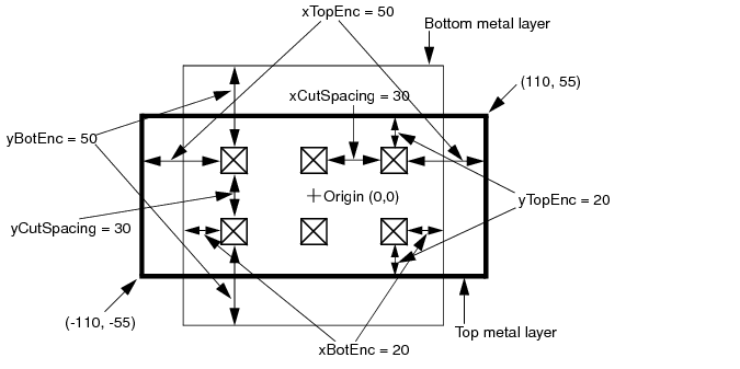
The same via rule with the following ORIGIN parameter shifts all of the metal and cut rectangles by 10 in the x direction, and by -10 in the y direction (see Figure 4-26 ):
+ ORIGIN 10 -10
Figure 4-26 Via Rule With Origin
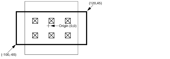
If the same via rule contains the following ORIGIN and OFFSET parameters, all of the rectangles shift by 10, -10. In addition, the top layer metal rectangle shifts by 20, -20, which means that the top metal shifts by a total of 30, -30.
+ ORIGIN 10 -10
+ OFFSET 0 0 20 -20
Figure 4-27 Via Rule With Origin and Offset
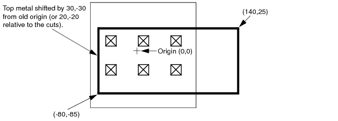
Example 4-37 Multi-Mask Patterns for Parameterized Vias with Via Rule
The following via rule describes a via cut mask pattern for a parameterized via:
+ VIARULE myGenVia1 + CUTSIZE 40 40
+ LAYERS M1 VIA1 M2 + CUTSPACING 40 40
+ ENCLOSURE 40 0 0 40 + ROWCOL 3 4
+ PATTERN 2_F_1_D ; #1 cut in top row is missing
Figure 4-28 Multi-Mask Patterns for Parameterized Vias
Figure 4-29 Multi-Mask Patterns for Parameterized Vias using Suffixes
For a fixed via specified using RECT or POLYGON statements, the cut shapes must either be all colored or uncolored. If the cuts are not colored, they will be automatically colored in a checkerboard pattern as shown in Figure 4-28. Each via cut with the same lower-left Y value is considered as one row, and each via in one row is a new column. For common "array" style vias with no missing cuts, this coloring is a good one. For vias that do not have a row and column structure or are missing cuts, then this coloring may not be good (see Figure 4-30 ). If the metal layers are not colored, some applications will color them to mask 1 for internal consistency, even though the via master metal shape colors are not really used by LEF or DEF via instances.
Example 4-38 Multi-Mask Patterns for Fixed Via
The following example shows a fixed-via with pre-colored cut shapes:
+ RECT M1 ( -40 -20 ) ( 120 20 ) #no mask, some readers set to 1
+ RECT VIA1 + MASK 1 ( -20 -20 ) ( 20 20 ) #first cut on mask 1
+ RECT VIA1 + MASK 2 ( 60 -20 ) ( 100 20 ) #second cut on mask 2
+ RECT ( -20 -40 ) ( 100 40 ) #no mask, some readers set to 1
Figure 4-30 Multi-Mask Patterns for Fixed Via
See the Fills, Nets, and Special Nets routing statements to see how a via instance uses these via-master mask values.
The PATTERN syntax that defines rows uses the ROWCOL parameters to specify the cut array. If the row has more bits than the numCutCols value in the ROWCOL parameter for this via, the last bits are ignored. The number of rows defined must equal the numCutRows value in the ROWCOL parameter.
Figure 4-31 illustrates the following via cut pattern syntax:
- myVia
+ VIARULE myViaRule
...
+ ROWCOL 5 5
+ PATTERN 2_F0_2_F8_1_78 ;]
The last three bits of F0, F8, and 78 are ignored because only five bits are allowed in a row. Therefore, the following PATTERN syntax gives the identical pattern:
+ PATTERN 2_F7_2_FF_1_7F
Figure 4-32 illustrates the following via cut pattern syntax:
- myVia
+ VIARULE myViaRule
...
+ ROWCOL 5 14
+ PATTERN 2_FFE0_3_R4F ;
The R4F value indicates a repeat of four Fs. The last two bits of each row definition are ignored because only 14 bits allowed in each row.