
A symbolic layout is, in practice, made of only of three objects:
| Object | mbk | Explanation |
|---|---|---|
| Segments | phseg | Oriented segments with a width and an orientation. |
| VIAs & contacts | phvia | Boils down to just a point. |
| Big VIAs & Big Contacts | phvia | Point with a width and a height That is a rectangle of width by height centered on the VIA coordinates. |
Each of thoses objects is associated to a symbolic layer which will control how the object is translated in many real rectangles.
| mbk | Layer Name | Usable By | Usage |
|---|---|---|---|
| phseg | nwell | Segment | N Well |
| PWELL | Segment | P Well | |
| NDIF | Segment | N Diffusion | |
| PDIF | Segment | P Diffusion | |
| NTIE | Segment | N Tie | |
| PTIE | Segment | P Tie | |
| NTRANS | Segment | N transistor, in Alliance, a transistor is represented as a segment (it's grid). | |
| PTRANS | Segment | P transistor | |
| POLY | Segment | Polysilicium | |
| ALUx | Segment | Metal level x | |
| CALUx | Segment | Metal level x, that can be used by the upper hierarchical level as a connector. From the layout point of view it is the same as ALUx. | |
| TALUx | Segment | Blockage for metal level x. Will diseappear in the real layout as it is an information for the P&R tools only. | |
| phvia | CONT_BODY_N | VIA, BIGVIA | Contact to N Well |
| CONT_BODY_P | VIA, BIGVIA | Contact to P Well | |
| CONT_DIF_N | VIA, BIGVIA | Contact to N Diffusion | |
| CONT_DIF_P | VIA, BIGVIA | Contact to P Diffusion | |
| CONT_POLY | VIA, BIGVIA | Contact to polysilicium | |
| CONT_VIA | VIA, BIGVIA | Contact between metal1 and metal2 | |
| CONT_VIAx | VIA, BIGVIA | Contact between metal x and metal x+1. The index is the the one of the bottom metal of the VIA. | |
| C_X_N | VIA | N transistor corner, to build transistor bend. Not used anymore in recent technos | |
| C_X_P | VIA | P transistor corner, to build transistor bend. Not used anymore in recent technos |
Note
Not all association of object and symbolic layers are meaningful. For instance you cannot associate a contact to a NTRANS layer.
Note
The symbolic layer associated with blockages is prefixed by a T, for transparency, which may seems silly. It is for historical reasons, it started as a true transparency, but at some point we had to invert the meaning (blockage) with the rise of over-the-cell routing, but the name stuck...
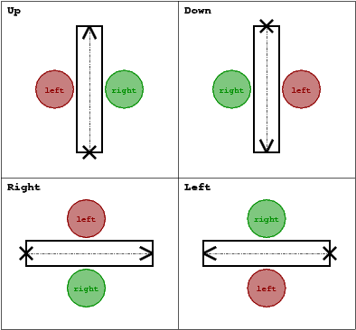
In Alliance, segments are oriented (up, down, left, right). This disambiguate the left or right side when using the LCW and RCW rules in the rds file. It allows to generate, if needed, asymetric object in the real layout file.
The RDS file control how a symbolic layout is transformed into it's real conterpart.
Note
Unit used inside the RDS file: all units are expressed in micrometers.
Alliance tools relying on the RDS file, and what layers are active for them:
| Tool | Name | RDS Flags |
|---|---|---|
| Layout editor | graal | ALL |
| Design Rule Checker | druc | ALL, drc |
| Electrical extractor | cougar | ALL, EXT |
| The symbolic to real layout translator | s2r | ALL |
RDS file:
DEFINE  PHYSICAL_GRID  0.005
DEFINE  LAMBDA         0.09
Tells that the physical grid (founder grid) step is 0.005µm and the lambda has a value of 0.09µm. That is, one lambda is 18 grid steps.
We can distinguish two kind of rds files:
The MBK_TO_RDS_SEGMENT table control the way segments are translated into real rectangles. Be aware that we are translating segments and not rectangles. Segments are defined by their axis (source & target points) and their width. The geometrical transformations are described according to that model. Obviously, they are either horizontal or vertical.
The translation method of a symbolic segment is as follow:
The segment is translated into one or more physical rectangles. The generated rectangles depends on the tool which is actually using rds and the flag for the considered real layer. For instance, real layers flagged with drc will be generated for s2r (for the cif or gds) and druc, but will not be shown under graal.
Translation into one real layer. First the source & target coordinates and width of the symbolic segment are multiplied by the LAMBDA value to obtain a real segment. Then one of the VW, LCW or RCW transformation is applied to that segment to get the final real rectangle.
VW for Variable Width, expand the real layer staying centered from the original one. In those rules, the third number is not used, it is only here to make the life easier for the parser...
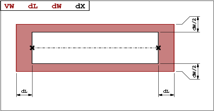
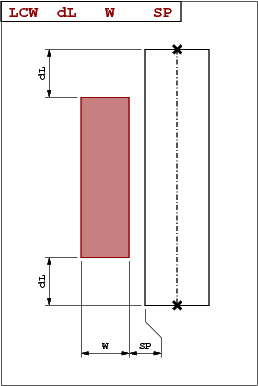
LCW or RCW for Left/Right Constant Width, create an off-center rectangle of fixed width relatively to the real segment. Note that the SP number is the distance between the edge of the real segment and the edge of the generated real rectangle (not from the axis). It is often zero.
Examples:
TABLE MBK_TO_RDS_SEGMENT

    # (Case 1)
    ALU1       RDS_ALU1   VW  0.18  0.09  0.0  ALL

    # (Case 2)
    NDIF       RDS_NDIF   VW  0.18  0.0   0.0  ALL \
               RDS_ACTIV  VW  0.18  0.0   0.0  DRC \
               RDS_NIMP   VW  0.36  0.36  0.0  DRC

    # (Case 3)
    NTRANS     RDS_POLY   VW  0.27  0.00  0.0  ALL \
               RDS_GATE   VW  0.27  0.00  0.0  DRC \
               RDS_NDIF  LCW  0.0   0.27  0.0  EXT \
               RDS_NDIF  RCW  0.0   0.27  0.0  EXT \
               RDS_NDIF   VW  0.0   0.72  0.0  DRC \
               RDS_ACTIV  VW  0.0   0.72  0.0  ALL \
               RDS_NIMP   VW  0.18  1.26  0.0  DRC

END
Case 1 the ALU1 is translated in exacltly one real rectangle of RDS_ALU1, both ends are extended by 0.18µm and it's width is increased by 0.09µm.
Case 2 the NDIF will be translated into only one segment under graal, for symbolic visualization. And into three real rectangles for s2r and druc.
Case 3 the NTRANS, associated to a transistor is a little bit more complex, the generated shapes are different for the extractor cougar in one hand, and for both druc & s2r in the other hand.
For the extractor (EXT & ALL flags) there will be four rectangles generateds:
As the extractor must kept separate the source and the drain of the transistor, they are generated as two offset rectangles, using the LCW and RCW directives.
For s2r and druc (drc and ALL), five rectangles are generateds:
In the layout send to the foundry, the source & drain are draw as one rectangle across the gate area (the transistor being defined by the intersection of both rectangles).
This table is to translate default VIAs into real via. In the symbolic layout the default VIA is simply a point and a set of layers. All layers are converted in squares shapes centered on the VIA coordinate. The one dimension given is the size of the side of that square.
Note that although we are refering to VIAs, which for the purists are between two metal layers, this table also describe contacts.
Example:
TABLE MBK_TO_RDS_VIA

    CONT_DIF_P RDS_PDIF  0.54 ALL \
               RDS_CONT  0.18 ALL \
               RDS_ALU1  0.36 ALL \
               RDS_ACTIV 0.54 DRC \
               RDS_PIMP  0.90 DRC

    CONT_POLY  RDS_POLY  0.54 ALL \
               RDS_CONT  0.18 ALL \
               RDS_ALU1  0.36 ALL

    CONT_VIA   RDS_ALU1  0.45 ALL \
               RDS_VIA1  0.27 ALL \
               RDS_ALU2  0.45 ALL

END
Note
In CONT_DIF_P you may see that only three layers will be shown under graal, but five will be generated in the gds layout.
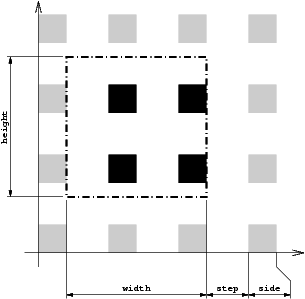
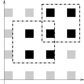
In s2r, when generating BIGVIAs, the matrix of holes they contains is not draw relative to the position of the BIGVIA itself, but on a grid which is common througout all the design real layout. This is to allow overlap between two BIGVIA without risking the holes matrix to be not exactly overlapping. As a consequence, when visualizing the gds file, the holes may not be centerend inside one individual BIGVIA.
The MBK_TO_RDS_BIGVIA_HOLE table define the global hole matrix for the whole design. The first number is the individual hole side and the second the grid step (edge to edge). The figure below show the hole generation.
Example of BIGVIA overlap:
Example:
TABLE MBK_TO_RDS_BIGVIA_HOLE

    CONT_VIA   RDS_VIA1 0.27 0.27 ALL
    CONT_VIA2  RDS_VIA2 0.27 0.27 ALL
    CONT_VIA3  RDS_VIA3 0.27 0.27 ALL
    CONT_VIA4  RDS_VIA4 0.27 0.27 ALL
    CONT_VIA5  RDS_VIA5 0.36 0.36 ALL

END
Note
BIGVIA demotion. If the size of the bigvia is too small, there is a possibility that no hole from the global matrix will be under it. To avoid that case, if the either side of the BIGVIA is less than 1.5 * step, the BIGVIA is demoted to a simple VIA.
This table describe how the metal part of a BIGVIA is expanded (for the hole part, see the previous table MBK_TO_RDS_BIGVIA_HOLE). The rule give for each metal:
Example:
TABLE MBK_TO_RDS_BIGVIA_METAL

    CONT_VIA  RDS_ALU1 0.0 0.09  ALL \
              RDS_ALU2 0.0 0.09  ALL

    CONT_VIA2 RDS_ALU2 0.0 0.09  ALL \
              RDS_ALU3 0.0 0.09  ALL

    CONT_VIA3 RDS_ALU3 0.0 0.09  ALL \
              RDS_ALU4 0.0 0.09  ALL

    CONT_VIA4 RDS_ALU4 0.0 0.09  ALL \
              RDS_ALU5 0.0 0.09  ALL

    CONT_VIA5 RDS_ALU5 0.0 0.09  ALL \
              RDS_ALU6 0.0 0.18  ALL
END
From a strict standpoint this table shouldn't be here but put in a separate configuration file, because it contains informations only used by the symbolic layout tools (ocp, nero, ring).
This table defines the cell gauge the routing pitch and minimal (symbolic) wire width and minimal spacing for the routers. They are patly redundant.
Example:
TABLE MBK_WIRESETTING

    X_GRID             10
    Y_GRID             10
    Y_SLICE           100
    WIDTH_VDD          12
    WIDTH_VSS          12
    TRACK_WIDTH_ALU8    0
    TRACK_WIDTH_ALU7    4
    TRACK_WIDTH_ALU6    4
    TRACK_WIDTH_ALU5    4
    TRACK_WIDTH_ALU4    3
    TRACK_WIDTH_ALU3    3
    TRACK_WIDTH_ALU2    3
    TRACK_WIDTH_ALU1    3
    TRACK_SPACING_ALU8  0
    TRACK_SPACING_ALU7  4
    TRACK_SPACING_ALU6  4
    TRACK_SPACING_ALU5  4
    TRACK_SPACING_ALU4  4
    TRACK_SPACING_ALU3  4
    TRACK_SPACING_ALU2  4
    TRACK_SPACING_ALU1  3

END