|
|
|||||||||
|
|
|
|
|
|
|
|
|
|
|
This chapter contains information about the following topics:
A Library Exchange Format (LEF) file contains library information for a class of designs. Library data includes layer, via, placement site type, and macro cell definitions. The LEF file is an ASCII representation using the syntax conventions described in "Typographic and Syntax Conventions".
Note the following information about creating LEF files:

|
Distance precision is controlled by the UNITS statement. |
|
|
LEF statements end with a semicolon ( ; ). You must leave a space between the last character in the statement and the semicolon. |
For information, see Character Information.
For information, see Name Escaping Semantics for Identifiers.
When reading in LEF files, always read in the technology LEF file first.
LEF files can contain the following statements. You can specify statements in any order; however, data must be defined before it is used. For example, the UNITS statement must be defined before any statements that use values that are dependent on UNITS values, LAYER statements must be defined before statements that use the layer names, and VIA statements must be defined before referencing them in other statements. If you specify statements in the following order, all data is defined before being used.
The following definitions describe the syntax arguments for the statements that make up a LEF file. Statements are listed in alphabetical order, not in the order they should appear in a LEF file. For the correct order, see "Order of LEF Statements".
BUSBITCHARS "[]" ;
If one of the bus bit characters appears in a LEF name as a regular character, you must use a backslash (\) before the character to prevent the LEF reader from interpreting the character as a bus bit delimiter.
If you do not specify the BUSBITCHARS statement in your LEF file, the default value is "[]".
Defines the clearance spacing requirement that will be applied to all object spacing in the SPACING and SPACINGTABLE statements. If you do not specify a CLEARANCEMEASURE statement, euclidean distance is used by default.
|
Uses the largest x or y distances for spacing between objects. |
|
|
Uses the euclidean distance for spacing between objects. That is, the square root of x2 + y2. |
DIVIDERCHAR "/" ;
If the divider character appears in a LEF name as a regular character, you must use a backslash (\) before the character to prevent the LEF reader from interpreting the character as a hierarchy delimiter.
If you do not specify the DIVIDERCHAR statement in your LEF file, the default value is "/".
Specifies the contents of the extension.
Identifies the extension block. You must enclose tag in double quotation marks.
Example 1-1 Extension Statement
CREATOR "company name"
DATE "timestamp"
REVISION "revision number"
Does not allow mask shifting. All the LEF macro pin mask assignments must be kept fixed and cannot be shifted to a different mask. The LEF macro pin shapes should all have MASK assignments, if FIXEDMASK is present. This statement should be included before the LAYER statements.
...
MANUFACTURINGGRID 0.001 ;
FIXEDMASK ;
LAYER xxx
You must define layers in process order from bottom to top. For example:
poly masterslice
cut01 cut
metal1 routing
cut12 cut
metal2 routing
cut23 cut
metal3 routing
Specifies how much AC current a cut of a certain area can handle at a certain frequency. For an example using the ACCURRENTDENSITY syntax, see Example 1-9.
The ACCURRENTDENSITY syntax is defined as follows:
{PEAK | AVERAGE | RMS}
{ value
| FREQUENCY freq_1 freq_2 ... ;
[CUTAREA cutArea_1 cutArea_2 ... ; ]
TABLEENTRIES
v_freq_1_cutArea_1 v_freq_1_cutArea_2 ...
v_freq_2_cutArea_1 v_freq_2_cutArea_2 ...
...
} ;
|
Specifies the root mean square limit of the layer. |
||
|
Specifies a maximum current limit for the layer in milliamps per square micron (mA/μm2). |
||
|
Specifies cut area values, in square microns (μm2). You can specify more than one cut area. If you specify multiple cut area values, the values must be specified in ascending order. |
||
|
Defines the maximum current for each frequency and cut area pair specified in the FREQUENCY and CUTAREA statements, in mA/μm2. The pairings define each cut area for the first frequency in the FREQUENCY statement, then the cut areas for the second frequency, and so on. The final value for a given cut area and frequency is computed from a linear interpolation of the table values. |
ANTENNAAREADIFFREDUCEPWL ( ( diffArea1 diffAreaFactor1 )
( diffArea2 diffAreaFactor2 ) ...)
Indicates that the cut_area is multiplied by a diffAreaFactor computed from a piece-wise linear interpolation, based on the diffusion area attached to the cut.
The diffArea values are floats, specified in microns squared. The diffArea values should start with 0 and monotonically increase in value to the maximum size diffArea possible. The diffAreaFactor values are floats with no units. The diffAreaFactor values are normally between 0.0 and 1.0. If no statement rule is defined, the diffMetalReduceFactor value in the PAR(mi) equation defaults to 1.0.
For more information on the PAR(mi) equation and process antenna models, see Appendix C, "Calculating and Fixing Process Antenna Violations."
ANTENNAAREAFACTOR value [DIFFUSEONLY]
Specifies the multiply factor for the antenna metal area calculation. DIFFUSEONLY specifies that the current antenna factor should only be used when the corresponding layer is connected to the diffusion.
Default: 1.0
Type: Float
For more information on process antenna calculation, see Appendix C, "Calculating and Fixing Process Antenna Violations."
Note: If you specify a value that is greater than 1.0, the computed areas will be larger, and violations will occur more frequently.
ANTENNAAREAMINUSDIFF minusDiffFactor
Indicates that the antenna ratio cut_area should subtract the diffusion area connected to it. This means that the ratio is calculated as:
ratio = (cutFactor x cut_area - minusDiffFactor x diff_area)/gate_area
If the resulting value is less than 0, it should be truncated to 0. For example, if a via2 shape has a final ratio that is less than 0 because it connects to a diffusion shape, then the cumulative check for metal3 (or via3) above the via2 shape adds a cumulative value of 0 from the via2 layer. (See Example 1 in Cut Layer Process Antenna Models, in Appendix C, "Calculating and Fixing Process Antenna Violations."
Type: Float
Default: 0.0
ANTENNAAREARATIO value
Specifies the maximum legal antenna ratio, using the area of the metal wire that is not connected to the diffusion diode. For more information on process antenna calculation, see Appendix C, "Calculating and Fixing Process Antenna Violations."
Type: Integer
ANTENNACUMAREARATIO value
Specifies the cumulative antenna ratio, using the area of the metal wire that is not connected to the diffusion diode. For more information on process antenna calculation, see Appendix C, "Calculating and Fixing Process Antenna Violations."
Type: Integer
ANTENNACUMDIFFAREARATIO {value | PWL ( ( d1 r1 ) ( d2 r2 )...)}
Specifies the cumulative antenna ratio, using the area of the metal wire that is connected to the diffusion diode. You can supply an explicit ratio value or specify piece-wise linear format (PWL), in which case the cumulative ratio is calculated using linear interpolation of the diffusion area and ratio input values. The diffusion input values must be specified in ascending order.
Type: Integer
For more information on process antenna calculation, see Appendix C, "Calculating and Fixing Process Antenna Violations."
Indicates that cumulative ratio rules (that is, ANTENNACUMAREARATIO, and ANTENNACUMDIFFAREARATIO) accumulate with the previous routing layer instead of the previous cut layer. Use this to combine metal and cut area ratios into one rule.
For more information on process antenna models, see Appendix C, "Calculating and Fixing Process Antenna Violations."
ANTENNADIFFAREARATIO {value | PWL ( ( d1 r1 ) ( d2 r2 )...)}
Specifies the antenna ratio, using the area of the metal wire connected to the diffusion diode. You can supply an explicit ratio value or specify piece-wise linear format (PWL), in which case the ratio is calculated using linear interpolation of the diffusion area and ratio input values. The diffusion input values must be specified in ascending order.
Type: Integer
For more information on process antenna calculation, see Appendix C, "Calculating and Fixing Process Antenna Violations."
ANTENNAGATEPLUSDIFF plusDiffFactor
Indicates the antenna ratio gate area includes the diffusion area multiplied by plusDiffFactor. This means that the ratio is calculated as:
ratio = cut_area / (gate_area + plusDiffFactor x diff_area)
The ratio rules without "DIFF" (the ANTENNAAREARATIO, ANTENNACUMAREARATIO, ANTENNASIDEAREARATIO, and ANTENNACUMSIDEAREARATIO statements), are unnecessary for this layer if ANTENNAGATEPLUSDIFF is defined because a zero diffusion area is already accounted for by the ANTENNADIFF*RATIO statements.
Type: Float
Default: 0.0
For more information on process antenna models, see Appendix C, "Calculating and Fixing Process Antenna Violations."
ANTENNAMODEL {OXIDE1 | OXIDE2 | OXIDE3 | OXIDE4}
Specifies the oxide model for the layer. If you specify an ANTENNAMODEL statement, that value affects all ANTENNA* statements for the layer that follow it until you specify another ANTENNAMODEL statement.
Default: OXIDE1, for a new LAYER statement
Because LEF is sometimes used incrementally, if an ANTENNA statement occurs twice for the same oxide model, the last value specified is used. For any given ANTENNA keyword, only one value or PWL table is stored for each oxide metal on a given layer.
For an example using the ANTENNAMODEL syntax, see Example 1-10.
Specifies array spacing rules to use on the cut layer. An array spacing rule is intended for large vias of size 3x3 or larger.
The ARRAYSPACING syntax is defined as follows:
[ARRAYSPACING [LONGARRAY]
[WIDTH viaWidth] CUTSPACING cutSpacing
{ARRAYCUTS arrayCuts
SPACING arraySpacing} ... ;
]
|
CUTSPACING cutSpacing |
||
|
Specifies the edge-of-cut to edge-of-cut spacing inside one cut array. |
||
|
ARRAYCUTS arrayCuts SPACING arraySpacing |
||
|
Indicates that a large via array with a size greater than or equal to arrayCuts x arrayCuts in both dimensions must use N x N cut arrays (where N = arrayCuts) separated from other cut arrays by a distance of greater than or equal to arraySpacing. For example, if arrayCuts = 3, then 2x3 and 2x4 arrays do not need to follow the array spacing rule. However, 3x3 and 3x4 arrays must follow the rule (3x4 is legal, if the LONGARRAY keyword is specified), while 4x4 or 4x5 arrays are violations, unless an arrayCuts = 4 rule is specified. (See Array Spacing Rule Example 1). If you specify multiple {ARRAYCUTS ...} statements, the arrayCuts values must be specified in increasing order. (See Array Spacing Rule Example 3.) |
||
|
Specifying more than one ARRAYCUTS statement creates multiple choices for via array generation. For example, you can define an arrayCuts = 4 rule with arraySpacing = 1.0, and an arrayCuts = 5 rule with arraySpacing = 1.5. Either rule is legal, and the application should choose which rule to use (presumably based on which rule produces the most via cuts in the given via area). |
||
|
Indicates that the via can use N x M cut arrays, where N = arrayCuts, and M can be any value, including one that is larger than N. (See Array Spacing Rule Example 2.) |
||
|
WIDTH viaWidth |
||
|
Indicates that the array spacing rules only apply if the via metal width is greater than or equal to viaWidth. (See Array Spacing Rule Example 1.) |
||
Example 1-2 Array Spacing Rules
Assume the following array spacing rule exists:
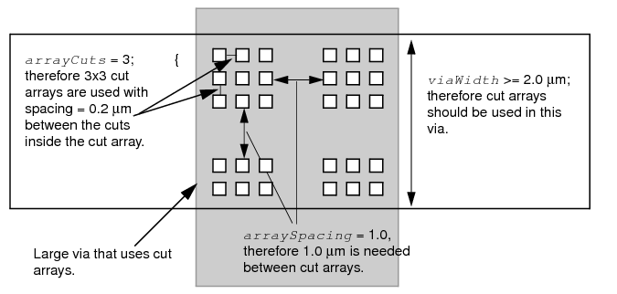
ARRAYSPACING WIDTH 2.0 CUTSPACING 0.2 ARRAYCUTS 3 SPACING 1.0 ;
Any via with a metal width greater than or equal to 2.0 μm should use the cut spacing of 0.2 μm between cuts inside 3x3 cut arrays, and the cut arrays should be spaced apart by a distance of greater than or equal to 1.0 μm from other cut arrays. This creates the via shown in Figure 1-1.
An array of 3x4 or 3x5 cuts spaced 0.2 μm apart is a violation, unless the LONGARRAY keyword is specified. This is because the 3x3 sub-array, inside 3x4 or 3x5 cut array, does not meet 1.0 μm spacing from other cut arrays. Also, any larger array, such as 4x4 or 4x5 cuts, is a violation because the 3x3 sub-array inside 4x4 or 4x5 cut array requires 1.0 μm spacing from other cut arrays.
Figure 1-1 Via Created With Array Spacing Width Rule
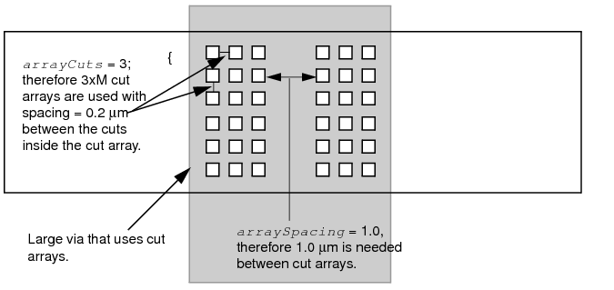
The following array spacing rule is the same as Example 1, except the LONGARRAY keyword is present and the WIDTH keyword is not specified, so it creates the via shown in Figure 1-2 :
ARRAYSPACING LONGARRAY CUTSPACING 0.2 ARRAYCUTS 3 SPACING 1.0 ;
An array of 2x2, 2x3, or 2xM cuts ignores this rule.
An array of 3x3 or 3xM must have 1.0 μm spacing from other cut arrays and 0.2 μm spacing between the cuts.
An array of 4x4 or 4xM is a violation because the array does not have 1.0 μm space from the 3xM sub-array inside the 4xM array.
Figure 1-2 Via Created With Array Spacing Long Array Rule
Assume the following multiple array spacing rules exist:
ARRAYSPACING LONGARRAY CUTSPACING 0.2
ARRAYCUTS 3 SPACING 1.0
ARRAYCUTS 4 SPACING 1.5
ARRAYCUTS 5 SPACING 2.0 ;
The application can choose between 3xM cut arrays with 1.0 μm spacing, 4xM cut arrays with 1.5 μm spacing, or 5xM cut arrays with 2.0 μm spacing, using 0.2 cut-to-cut spacing inside each cut array. No WIDTH value indicates that any via with more than three via cuts in both dimensions (that is, 3x3 and 3x4, but not 2x4) must follow these rules.
Specifies how much DC current a via cut of a certain area can handle in units of milliamps per square micron (mA/μm2). For an example using the DCCURRENTDENSITY syntax, see Example 1-11.
The DCCURRENTDENSITY syntax is defined as follows:
AVERAGE
{ value
| CUTAREA cutArea_1 cutArea_2 ... ;
TABLEENTRIES value_1 value_2 ...
} ;
|
Specifies a current limit for the layer in mA/μm2. |
||
|
Specifies the maximum current density for each specified cut area, in mA/μm2. The final value for a specific cut area is computed from a linear interpolation of the table values. |
Specifies an enclosure rule for the cut layer.
The ENCLOSURE syntax is described as follows:
[ENCLOSURE
[ABOVE | BELOW] overhang1 overhang2
[ WIDTH minWidth [EXCEPTEXTRACUT cutWithin]
| LENGTH minLength]
;]
|
ENCLOSURE [ABOVE | BELOW] overhang1 overhang2 |
||
|
Indicates that any rectangle from this cut layer requires the routing layers to overhang by overhang1 on two opposite sides, and by overhang2 on the other two opposite sides. (See Figure 1-3.) If you specify BELOW, the overhang is required on the routing layers below this cut layer. If you specify ABOVE, the overhang is required on the routing layers above this cut layer. If you specify neither, the rule applies to both adjacent routing layers. |
||
|
WIDTH minWidth |
||
|
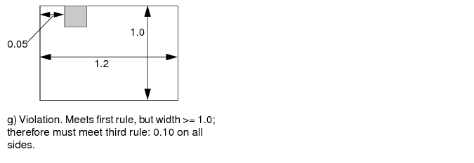
Indicates that the enclosure rule only applies when the width of the routing layer is greater than or equal to minWidth. If you do not specify a minimum width, the enclosure rule applies to all widths (as if minWidth equaled 0). If you specify multiple enclosure rules with the same width (or with no width), then there are several legal enclosure rules for this width, and the application only needs to meet one of the rules. If you specify multiple enclosure rules with different minWidth values, the largest minWidth rule that is still less than or equal to the wire width applies. For example, if you specify enclosure rules for 0.0 μm, 1.0 μm, and 2.0 μm widths, then a 0.5 μm wire must meet a 0.0 rule, a 1.5 μm wire must meet a 1.0 rule, and a 2.0 μm wire must meet a 2.0 rule. (See Example 1-3.) |
||
|
EXCEPTEXTRACUT cutWithin |
||
|
Indicates that if there is another via cut having same metal shapes on both metal layers less than or equal to cutWithin distance away, this ENCLOSURE with WIDTH rule is ignored and the ENCLOSURE rules for minimum width wires (that is, no WIDTH keyword) are applied to the via cuts instead. (See Example 1-4.) |
||
|
LENGTH minLength |
||
|
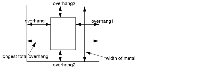
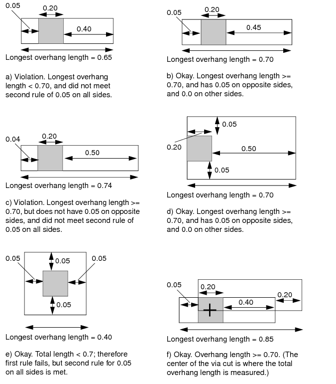
Indicates that the enclosure rule only applies if the total length of the longest opposite-side overhangs is greater than or equal to minLength. The total length of the overhang is measured at the via cut center (see illustration F in Figure 1-5 ). |
||
Figure 1-3 Enclosure Rule
Example 1-3 Enclosure Rules
|
|
The following definition describes a cut layer that has different enclosure rules for m1 below than for m2 above. |
LAYER via12
TYPE CUT ;
WIDTH 0.20 ; #cuts .20 x .20 squares
ENCLOSURE BELOW .03 .01 ; #m1: 0.03 on two opposite sides, 0.01 on other
ENCLOSURE ABOVE .05 .01 ; #m2: 0.05 on two opposite sides, 0.01 on other
RESISTANCE 10.0 ; #10.0 ohms per cut
...
END via12
LAYER via23
TYPE CUT ;
WIDTH 0.20 ; #cuts .20 x .20 squares
SPACING 0.15 #via23 edge-to-edge spacing is 0.15
ENCLOSURE .05 .01 ; #m2, m3: 0.05 on two opposite sides, 0.01 on
#other sides
ENCLOSURE .02 .02 WIDTH 1.0 ; #m2 needs 0.02 on all sides if m2 width >=1.0
#m3 needs 0.02 on all sides if m3 width >=1.0
ENCLOSURE .05 .05 WIDTH 2.0 ; #m2 needs 0.05 on all sides if m2 width >=2.0
#m3 needs 0.05 on all sides if m3 width >=2.0
...
END via23
|
|
The following definition describes a cut layer that requires an overhang of .07 μm on all sides of metal3, and an overhang of .09 μm on all sides of metal4, if the widths of metal3 and metal4 are greater than or equal to 1.0 μm: |
LAYER via34
TYPE CUT ;
WIDTH 0.25 ; #cuts .25 x .25 squares
ENCLOSURE .05 .01 ; #minimum width enclosure rule
ENCLOSURE BELOW .07 .07 WIDTH 1.0 ; #m3 needs .07 on all sides if m3 width >=1.0
ENCLOSURE ABOVE .09 .09 WIDTH 1.0 ; #m4 needs .09 on all sides if m4 width >=1.0
...
END via34
Example 1-4 Enclosure Rule With Width and ExceptExtraCut
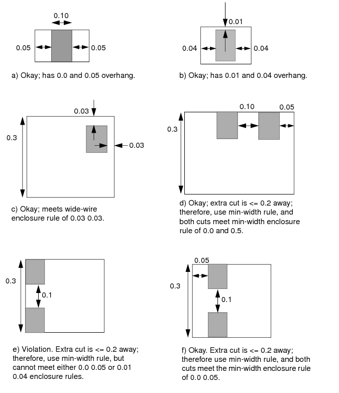
The following definition describes a cut layer that requires an enclosure of either .05 μm on opposite sides and 0.0 μm on the other two sides, or 0.04 μm on opposites sides and 0.01 μm on the other two sides. It also requires an enclosure of 0.03 μm in all directions if the wire width is greater than or equal to 0.03 μm, unless there is an extra cut (redundant cut) within 0.2 μm.
WIDTH 0.10 #cuts .10 x .10 squares
SPACING 0.10 ; #minimum edge-to-edge spacing is 0.10
ENCLOSURE 0.0 0.05 ; #overhang 0.0 0.05
ENCLOSURE 0.01 0.04 ; #or, overhang 0.01 0.04
#if width >= 0.3, need 0.03 0.03, unless extra cut across wire within 0.2μm
ENCLOSURE 0.03 0.03 WIDTH 0.3 EXCEPTEXTRACUT 0.2 ;
Figure 1-4 Illustrations of Enclosure Rule With Width and ExceptExtraCut
Example 1-5 Enclosure Rule With Length and Width
The following definition describes a cut layer that requires an enclosure of .05 μm on opposite sides and 0.0 μm on the other two sides, as long as the total length enclosure on any two opposite sides is greater than or equal to 0.7 μm. Otherwise, it requires 0.05 μm on all sides if the total enclosure length is less than or equal to 0.7 μm. It also requires 0.10 μm on all sides if the metal layer has a width that is greater than or equal to 1.0 μm. (Figure 1-5 illustrates examples of violations and acceptable vias for the three ENCLOSURE rules.)
WIDTH 0.20 #cuts .20 x .20 squares
SPACING 0.20 ; #via34 edge-to-edge spacing is 0.20
ENCLOSURE 0.05 0.0 LENGTH 0.7 ; #overhang 0.05 0.0 if total overhang >= 0.7
ENCLOSURE 0.05 0.05 ; #or, overhang 0.05 on all sides
ENCLOSURE 0.10 0.10 WIDTH 1.0 ; #if width >= 1.0, always need 0.10
Figure 1-5 Illustrations of Enclosure Rule With Length and Width
LAYER LayerName
Specifies the name for the layer. This name is used in later references to the layer.
MASK maskNum
Specifies how many masks for double- or triple-patterning will be used for this layer. The maskNum variable must be an integer greater than or equal to 2. Most applications support values of 2 or 3 only.
PREFERENCLOSURE [ABOVE | BELOW] overhang1 overhang2 [WIDTH minWidth]
Specifies preferred enclosure rules that can improve manufacturing yield, instead of enclosure rules that absolutely must be met (see the ENCLOSURE keyword). Applications should use the PREFERENCLOSURE rule when it has little or no impact on density and routability.
PROPERTY propName propVal
Specifies a numerical or string value for a layer property defined in the PROPERTYDEFINITIONS statement. The propName you specify must match the propName listed in the PROPERTYDEFINITIONS statement.
RESISTANCE resistancePerCut
Specifies the resistance per cut on this layer. LEF vias without their own specific resistance value, or DEF vias from a VIARULE without a resistance per cut value, can use this resistance value.
Via resistance is computed using resistancePerCut and Kirchoff's law for typical parallel resistance calculation. For example, if R =10 ohms per cut, and the via has one cut, then R =10 ohms. If the via has two cuts, then R = (1/2) * 10 = 5 ohms.
Specifies the minimum spacing allowed between via cuts on the same net or different nets. For via cuts on the same net, this value can be overridden by a spacing with the SAMENET keyword. (See Example 1-6.)
The SPACING syntax is defined as follows:
[SPACING cutSpacing
[CENTERTOCENTER]
[SAMENET]
[ LAYER secondLayerName [STACK]
| ADJACENTCUTS {2 | 3 | 4} WITHIN cutWithin
[EXCEPTSAMEPGNET]
| PARALLELOVERLAP
| AREA cutArea]
;] ...
|
Specifies the default minimum spacing between via cuts, in microns. |
||
|
Computes the cutSpacing or cutWithin distances from cut-center to cut-center, instead of from cut-edge to cut-edge (the default behavior). (See Spacing Rule Example 4.) |
||
|
Indicates that the cutSpacing value only applies to same-net cuts. The SAMENET cutSpacing value should be smaller than the normal SPACING cutSpacing value that applies to different-net cuts. |
||
|
LAYER secondLayerName |
||
|
Applies the spacing rule between objects on the cut layer and objects on 2ndLayerName. The second layer must be a cut or routing layer already defined in the LEF file, or the next routing layer declared in the LEF file. This allows "one layer look ahead," which is needed in some technologies. (See Spacing Rule Example 1.) |
||
|
Indicates that same-net cuts on two different layers can be stacked if they are aligned. If the cuts are not the same size, the smaller cut must be completely covered by the larger cut, to be considered legal. If both cuts are the same size, the centers of the cuts must be aligned, to be legal; otherwise, the cuts must have cutSpacing between them. If cutSpacing is 0.0, the same-net cut vias can be placed anywhere legally, including slightly overlap case. (See Spacing Rule Example 7.) Most applications only allow spacing checks and STACK checking if secondLayerName is the cut layer below the current cut layer. |
||
|
ADJACENTCUTS {2 |3 | 4} WITHIN cutWithin |
||
|
Applies the spacing rule only when the cut has two, three, or four via cuts that are less than cutWithin distance, in microns, from each other. You can specify only one ADJACENTCUTS statement per cut layer. For more information, see "Adjacent Via Cuts." |
||
|
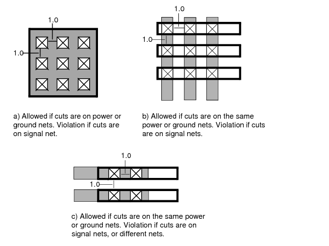
Indicates that the ADJACENTCUTS rule does not apply between cuts, if they are on the same net, and are on a power or ground net. (See Spacing Rule Example 5.) |
||
|
Indicates that cuts on different metal shapes that have a parallel edge overlap greater than 0 require cutSpacing distance between them. Only one PARALLELOVERLAP spacing value is allowed per cut layer. The rule does not apply to cuts that share the same metal shapes above or below that cover the overlap area between the cuts. (See Spacing Rule Example 8.) |
||
|
AREA cutArea |
||
|
Indicates that any cut with an area greater than or equal to cutArea requires edge-to-edge spacing greater than or equal to cutSpacing to all other cuts. (See Spacing Rule Example 6.) A SPACING statement should already exist that applies to all cuts. Only cuts that have area greater than or equal to cutArea require extra spacing; therefore, cutSpacing for this keyword must be greater than the default spacing. If you include CENTERTOCENTER, the cutSpacing values are computed from cut-center to cut-center, instead of from cut-edge to cut-edge. |
||
Example 1-6 Spacing Rule Examples
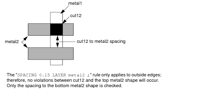
The following spacing rule defines the cut spacing required between a cut and the routing immediately above the cut. The spacing only applies to "outside edges" of the routing shape, and does not apply to a routing shape already overlapping the cut shape.
LAYER cut12
SPACING 0.10 ; #normal min cut-to-cut spacing
SPACING 0.15 LAYER metal2 ; #spacing from cut to routing edge above
...
END cut12
LAYER metal2
...
END metal2
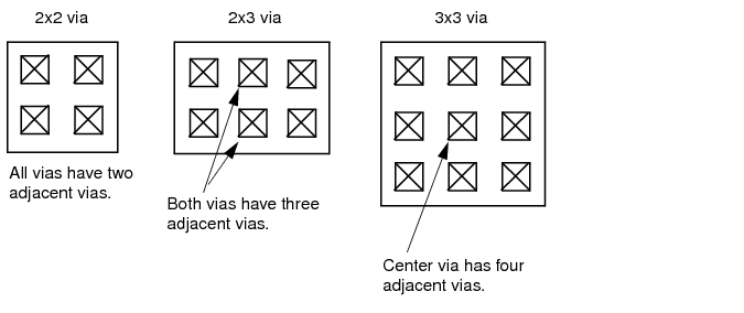
The following spacing rule specifies that extra space is needed for any via with more than three adjacent cuts, which happens if one via has more than 2x2 cuts (see Figure 1-6 ). A cut that is within .25 μm of three other cuts requires spacing that is greater than or equal to 0.22 μm.
LAYER CUT12
SPACING 0.20 ; #default cut spacing
SPACING 0.22 ADJACENTCUTS 3 WITHIN 0.25 ;
...
END CUT12
Adjacent Via Cuts
A cut is considered adjacent if it is within distance of another cut in any direction (including a 45-degree angle). Figure 1-6 illustrates adjacent via cuts for 2x2, 2x3, and 3x3 vias, for typical spacing values (that is, the diagonal spacing is greater than the ADJACENTCUTS distance value). For three adjacent cuts, the ADJACENTCUTS rule allows tight cut spacing on 1xn vias and 2x2 vias, but requires larger cut spacing on 2x3, 2x4 and 3xn vias. For four adjacent cuts, the rule allows tight cut spacing on 2xn vias, but it requires larger cut spacing on 3xn vias.
The ADJACENTCUTS rule overrides the cut-to-cut spacing used in VIARULE GENERATE statements for large vias if the ADJACENTCUTS spacing value is larger than the VIARULE spacing value.
The following spacing rule specifies that extra space is required for any via with 3x3 cuts or more (that is, a cut with four or more adjacent cuts - see Figure 1-6 ). A cut that is within .25 μm of four other cuts requires spacing that is greater than or equal to 0.22 μm.
LAYER CUT12
SPACING 0.20 ; #default cut spacing
SPACING 0.22 ADJACENTCUTS 4 WITHIN 0.25 ;
...
END CUT12
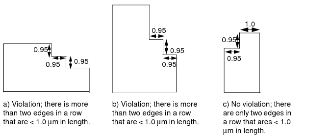
The following spacing rule indicates that center-to-center spacing of greater than or equal to 0.30 μm is required if the center-to-center spacing to three or more cuts is less than 0.30 μm. This is equivalent to saying a cut can have only two other cuts with center-to-center spacing that is less than 0.30 μm.
SPACING 0.30 CENTERTOCENTER ADJACENTCUTS 3 WITHIN 0.30 ;
Figure 1-7 illustrates the following spacing rule:
SPACING 1.0 ;
SPACING 1.2 ADJACENTCUTS 2 WITHIN 1.5 EXCEPTSAMEPGNET ;
Figure 1-7 Except Same PG Net Rule
The following spacing rule indicates that normal cuts require 0.10 μm edge-to-edge spacing, and cuts with an area greater than or equal to 0.02 μm2 require 0.12 μm edge-to-edge spacing to all other cuts:
SPACING 1.0 ;
SPACING 0.12 AREA 0.02 ;
The following spacing rule indicates cut23 cuts must be 0.20 μm from cut12 cuts unless they are exactly aligned:
LAYER cut23 ;
SPACING 0.20 SAMENET LAYER cut12 STACK ;
Figure 1-8 illustrates the following spacing rule:
SPACING 1.0 ;
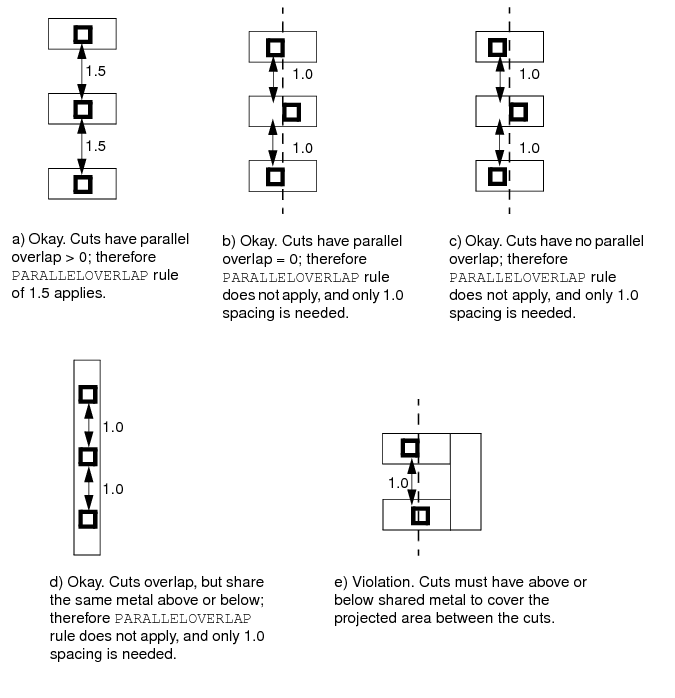
SPACING 1.5 PARALLELOVERLAP ;
Figure 1-8 Parallel Overlap Rule
Specifies spacing tables to use on the cut layer.
The SPACINGTABLE syntax is defined as follows:
SPACINGTABLE ORTHOGONAL
{WITHIN cutWithin SPACING orthoSpacing}...
;]
|
WITHIN cutWithin SPACING orthoSpacing |
||
|
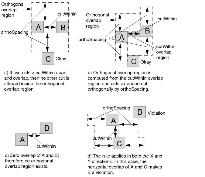
Indicates that if two cuts have parallel overlap that is greater than 0, and they are less than cutWithin distance from each other, any other cuts in an orthogonal direction must have greater than or equal to orthoSpacing. (See Example 1-6 , and Figure 1-9.) |
||
Example 1-7 Spacing Table Orthogonal Rule
The following example shows how a spacing table orthogonal rule is defined:
SPACING 0.10 #min spacing for all cuts
Figure 1-9 Spacing Table Orthogonal Overlap Regions
Specifies that the layer is for contact-cuts. The layer is later referenced in vias, and in rules for generating vias.
WIDTH minWidth
Specifies the minimum width of a cut. In most technologies, this is also the only legal size of a cut.
Type: Float, specified in microns
|
LAYER layerName |
Specifies the name for the layer. This name is used in later references to the layer. |
|
LAYER layerName2 |
Specifies the name of another implant layer that requires extra spacing that is greater than or equal to minspacing from this implant layer. |
|
MASK maskNum |
Specifies how many masks for double- or triple-patterning will be used for this layer. The maskNum variable must be an integer greater than or equal to 2. Most applications only support values of 2 or 3. |
|
PROPERTY propName propVal |
|
|
Specifies a numerical or string value for a layer property defined in the PROPERTYDEFINITIONS statement. The propName you specify must match the propName listed in the PROPERTYDEFINITIONS statement. |
|
|
SPACING minSpacing |
|
|
Specifies the minimum spacing for the layer. This value affects the legal cell placement. |
|
|
WIDTH minWidth |
Specifies the minimum width for this layer. This value affects the legal cell placement. |
Example 1-8 Implant Layer
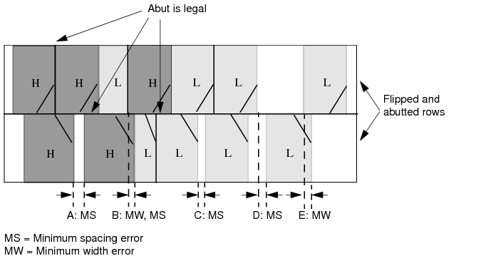
Typically, you define high-drive cells on one implant layer and low-drive cells on another implant layer. The following example defines high-drive cells on implant1 and low-drive cells on implant2. Both implant layers cover the entire cell. The placer and filler cell creation attempt to legalize the cell overlaps in abutting rows to ensure that the minimum width and spacing values are met.
LAYER implant1 #high-drive implant layer
TYPE IMPLANT ;
WIDTH 0.50 ; #implant rectangles must be >=0.50 microns wide
SPACING 0.50 ; #implant rectangles must be >=0.50 microns apart
LAYER implant2 #low-drive implant layer
TYPE IMPLANT ;
WIDTH 0.50 ; #implant rectangles must be >=0.50 microns wide
SPACING 0.50 ; #implant rectangles must be >=0.50 microns apart
Assume that the high-drive cells and low-drive cells are completely covered by their respective implant layers. Because there is no spacing between implant1 and implant2 specified, you might see a placement like that illustrated in Figure 1-10.
Defines masterslice (nonrouting) or overlap layers in the design. Masterslice layers are typically polysilicon layers and are only needed if the cell MACROs have pins on the polysilicon layer.
The overlap layer should normally be named OVERLAP. It can be used in MACRO definitions to form rectilinear-shaped cells and blocks (that is, an "L"-shaped block).
You must define layers in process order from bottom to top. For example:
poly masterslice
cut01 cut
metal1 routing
cut12 cut
metal2 routing
cut23 cut
metal3 routing
LAYER layerName
Specifies the name for the layer. This name is used in later references to the layer.
Specifies the purpose of the layer.
MASK maskNum
Specifies how many masks for double- or triple-patterning will be used for this layer. The maskNum variable must be an integer greater than or equal to 2. Most applications only support values of 2 or 3.
PROPERTY propName propVal
Specifies a numerical or string value for a layer property defined in the PROPERTYDEFINITIONS statement. The propName you specify must match the propName listed in the PROPERTYDEFINITIONS statement.
A type rule can be used to further classify a masterslice layer.
You can create a type rule by using the following property definition:
|
Defines a special masterslice layer that is used to define the areas of a region on which a set of rules defined in the metal, cut, and/or trim metal layers with the REGION property would be applied. |
|
|
Defines a trim metal layer. This layer type is only used along with metal layers manufactured with self-aligned double patterning (SADP) technology. The TRIMMETAL layer has the shapes for the SADP mask used to "trim" or "cut" or "block" the self-aligned metal lines created during the first mask step of SADP processing. These shapes could be pre-defined in macros/cells or added at the line-end of a wires during routing. There are additional rules in cut and metal layers to define constraints to those shapes on a TRIMMETAL layer. |
|
|
|
The following example indicates that macro A defines a region of (0,0) to (100, 100) with respect to the placement of that macro, such that the boundary of the above die does not overlap: |
LAYER TOPDIE
TYPE MASTERSLICE
PROPERTY LEF58_TYPE "TYPE ABOVEDIEEDGE ;" ;
END TOPDIE
MACRO A
...
OBS
LAYER TOPDIE
RECT 0.000 0.000 100.000 100.000 ;
END
...
END A
Trimmed metal rules can be used to specify the metal layer that the shapes on the TRIMMETAL layer tries to trim.
You can create a trimmed metal rule by using the following property definition:
|
TRIMMEDMETAL metalLayer [MASK maskNum] |
|
|
Specifies the metal layer metalLayer that the shapes on the TRIMMETAL layer tries to trim. If maskNum is given, only maskNum on metalLayer is trimmed. |
|
|
|
The following is an example of a double patterned layer TM1 used to trim both masks of M1. As both TM1 and M1 are double-patterned, and the TRIMMEDMETAL property does not specify a mask, it implies that MASK 1 of TM1 trims MASK 1 of M1, and MASK 2 of TM1 trims MASK 2 of M1. |
LAYER TM1
TYPE MASTERSLICE ;
MASK 2 ;
PROPERTY LEF58_TYPE "TYPE TRIMMETAL ; " ;
PROPERTY LEF58_TRIMMEDMETAL "TRIMMEDMETAL M1 ; " ;
...
END TM1
...
LAYER M1
TYPE ROUTING ;
MASK 2 ;
...
END M1
|
|
The following example is of a single patterned TRIMMETAL TM2 layer, which trims only one mask of the double-patterned M2 layer. This is indicated by the MASK 1 portion of TM2's TRIMMEDMETAL property: |
LAYER TM2
TYPE MASTERSLICE ;
PROPERTY LEF58_TYPE "TYPE TRIMMETAL ; " ;
PROPERTY LEF58_TRIMMEDMETAL "TRIMMEDMETAL M2 MASK 1 ; " ;
...
END TM2
LAYER M2
TYPE ROUTING ;
MASK 2 ;
...
END M2
You must define layers in process order from bottom to top. For example:
poly masterslice
cut01 cut
metal1 routing
cut12 cut
metal2 routing
cut23 cut
metal3 routing
Specifies how much AC current a wire on this layer of a certain width can handle at a certain frequency in units of milliamps per micron (mA/μm).
Note: The true meaning of current density would have units of milliamps per square micron (mA/μm2); however, the thickness of the metal layer is implicitly included, so the units in this table are milliamps per micron, where only the wire width varies.
The ACCURRENTDENSITY syntax is defined as follows:
{PEAK | AVERAGE | RMS}
{ value
| FREQUENCY freq_1 freq_2 ... ;
[WIDTH width_1 width_2 ... ; ]
TABLEENTRIES
v_freq_1_width_1 v_freq_1_width_2 ...
v_freq_2_width_1 v_freq_2_width_2 ...
...
} ;
|
Specifies the root mean square current limit of the layer. |
||
|
Specifies a maximum current for the layer in mA/μm. |
||
|
Defines the maximum current for each of the frequency and width pairs specified in the FREQUENCY and WIDTH statements, in mA/μm. The pairings define each width for the first frequency in the FREQUENCY statement, then the widths for the second frequency, and so on. |
Example 1-9 AC Current Density Statements
Most LEF files do not include PEAK or AVERAGE limits. The PEAK limits are not a practical problem for digital signal routing. The AVERAGE limits are only needed for DC limits and not AC currents.
Most technologies do not have frequency dependency for RMS limits, but the LEF syntax requires a frequency value, so in practice the frequency value is a single value of 1, as shown in the example below. In this case the RMS limit does not vary with the frequency.
The following examples define AC current density tables:
The RMS current density at 0.7 μm is 9.0 + (7.5 - 9.0) x (0.8 - 0.7) / (0.8 - 0.4) = 8.625 mA/μm at frequency 300Mhz. Therefore, a 0.7 μm wide wire can carry 8.625 x 0.7 = 6.035 mA of RMS current.
The RMS current density at 0.7 μm is 7.5 + (6.8 - 7.5) x (0.8 - 0.7) / (0.8 - 0.4) = 7.325 mA/μm at frequency 600Mhz. Therefore, a 0.7 μm wide wire can carry 7.325 x 0.7 = 5.1275 mA of RMS current.
...
ACCURRENTDENSITY PEAK #peak AC current limit for met1
FREQUENCY 100 400 ; #2 freq values in MHz
WIDTH
0.4 0.8 1.6 5.0 10.0 ; #5 width values in microns
TABLEENTRIES
9.0 7.5 6.5 5.4 4.7 #mA/um for 5 widths and freq_1 (when the frequency #is 100 Mhz)
7.5 6.8 6.0 4.8 4.0 ; #mA/um for 5 widths and freq_2 (when the frequency #is 400 Mhz)
The PEAK current density at 0.7 μm for 100 Mhz is 9.0 + (7.5 - 9.0) x (0.8 - 0.7) / (0.8 - 0.4) = 8.625 mA/μm, and at 0.7 μm for 400 Mhax is 7.5 + (6.8 - 7.5) x (0.8 - 0.7) / (0.8 - 0.4) = 7.325 mA/mm. Then interpolating between the frequencies at 300Mhz gives 8.625 + (7.325 - 8.625) x (400 - 300) / (400 - 100) = 8.192 mA/μm.
The RMS current density at 0.4 μm is 7.5 mA/μm. Therefore, a 0.4 μm wide wire can carry 7.5 x .4 = 3.0 μm of RMS current.
...
ACCURRENTDENSITY PEAK #peak AC current limit for one cut
FREQUENCY 10 200 ; #2 freq values in MHz
CUTAREA 0.16 0.32 ; #2 cut areas in um squared
TABLEENTRIES
0.5 0.4 #mA/um squared for 2 cut areas at freq_1 (10 Mhz)
0.4 0.35 ; #mA/um squared for 2 cut areas at freq_2 (200 Mhz)
ACCURRENTDENSITY AVERAGE #average AC current limit for via cut12
10.0 ; #mA/um squared for any cut area at any frequency
ACCURRENTDENSITY RMS #RMS AC current limit for via cut12
FREQUENCY 1 ; #1 freq (required by syntax; not really used)
CUTAREA 0.16 1.6 ; #2 cut areas in um squared
TABLEENTRIES
10.0 9.0 ; #mA/um squared for 2 cut areas at any frequency
....
ANTENNAAREADIFFREDUCEPWL ( ( diffArea1 diffMetalFactor1 )
( diffArea2 diffMetalFactor2 ) ...)
Indicates that the metal area is multiplied by a diffMetalReduceFactor that is computed from a piece-wise linear interpolation based on the diff_area attached to the metal. (See Example 4 in Appendix C, "Calculating and Fixing Process Antenna Violations.") This means that the ratio is calculated as:
ratio = (metalFactor x metal_area x diffMetalReduceFactor) / gate_area
The diffArea values are floats, specified in microns squared. The diffArea values should start with 0 and monotonically increase in value to the maximum size diffArea allowed. The diffMetalFactor values are floats with no units. The diffMetalFactor values are normally between 0.0 and 1.0. If no rule is defined, the diffMetalReduceFactor value in the PAR(mi) equation defaults to 1.0.
For more information on the PAR(mi) equation and process antenna models, see Appendix C, "Calculating and Fixing Process Antenna Violations."
ANTENNAAREAFACTOR value [DIFFUSEONLY]
Specifies the multiply factor for the antenna metal area calculation. DIFFUSEONLY specifies that the current antenna factor should only be used when the corresponding layer is connected to the diffusion.
Default: 1.0
Type: Float
For more information on process antenna calculation, see Appendix C, "Calculating and Fixing Process Antenna Violations."
Note: If you specify a value that is greater than 1.0, the computed areas will be larger, and violations will occur more frequently.
ANTENNAAREAMINUSDIFF minusDiffFactor
Indicates that the antenna ratio metal area should subtract the diffusion area connected to it. This means that the ratio is calculated as:
ratio = (metalFactor x metal_area - minusDiffFactor x diff_area) /gate_area
If the resulting value is less than 0, it should be truncated to 0. For example, if a metal2 shape has a final ratio that is less than 0 because it connects to a diffusion shape, then the cumulative check for metal3 (or via2) connected to the metal2 shape adds in a cumulative value of 0 from the metal2 layer. (See Example 1 in Appendix C, "Calculating and Fixing Process Antenna Violations.")
Type: Float
Default: 0.0
For more information on process antenna models, see Calculating a PAR, in Appendix C, "Calculating and Fixing Process Antenna Violations."
ANTENNAAREARATIO value
Specifies the maximum legal antenna ratio, using the area of the metal wire that is not connected to the diffusion diode. For more information on process antenna calculation, see Appendix C, "Calculating and Fixing Process Antenna Violations."
Type: Integer
ANTENNACUMAREARATIO value
Specifies the cumulative antenna ratio, using the area of the wire that is not connected to the diffusion diode. For more information on process antenna calculation, see Appendix C, "Calculating and Fixing Process Antenna Violations."
Type: Integer
ANTENNACUMDIFFAREARATIO {value | PWL ( ( d1 r1 ) ( d2 r2 )...)}
Specifies the cumulative antenna ratio, using the area of the metal wire that is connected to the diffusion diode. You can supply and explicit ratio value or specify piece-wise linear format (PWL), in which case the cumulative ratio value is calculated using linear interpolation of the diffusion area and ratio input values. The diffusion input values must be specified in ascending order.
Type: Integer
For more information on process antenna calculation, see Appendix C, "Calculating and Fixing Process Antenna Violations."
ANTENNACUMDIFFSIDEAREARATIO {value | PWL ( ( d1 r1 ) ( d2 r2 )...)}
Specifies the cumulative antenna ratio, using the side wall area of the metal wire that is connected to the diffusion diode. You can supply and explicit ratio value or specify piece-wise linear format (PWL), in which case the cumulative ratio value is calculated using linear interpolation of the diffusion area and ratio input values. The diffusion input values must be specified in ascending order.
Type: Integer
For more information on process antenna calculation, see Appendix C, "Calculating and Fixing Process Antenna Violations."
Indicates that the cumulative ratio rules (ANTENNACUMAREARATIO and ANTENNACUMDIFFAREARATIO) accumulate with the previous cut layer instead of the previous metal layer. Use this to combine metal and cut area ratios into one cumulative ratio rule.
Note: This rule does not affect ANTENNACUMSIDEAREARATIO and ANTENNACUMDIFFSIDEAREA models.
For more information on process antenna models, see Calculating a CAR, in Appendix C, "Calculating and Fixing Process Antenna Violations."
ANTENNACUMSIDEAREARATIO value
Specifies the cumulative antenna ratio, using the side wall area of the metal wire that is not connected to the diffusion diode. For more information on process antenna calculation, see Appendix C, "Calculating and Fixing Process Antenna Violations."
ANTENNADIFFAREARATIO {value | PWL ( ( d1 r1 ) ( d2 r2 )...)}
Specifies the antenna ratio, using the area of the metal wire that is connected to the diffusion diode. You can supply and explicit ratio value or specify piece-wise linear format (PWL), in which case the ratio value is calculated using linear interpolation of the diffusion area and ratio input values. The diffusion input values must be specified in ascending order.
Type: Integer
For more information on process antenna calculation, see Appendix C, "Calculating and Fixing Process Antenna Violations."
ANTENNADIFFSIDEAREARATIO {value | PWL ( ( d1 r1 ) ( d2 r2 )...)}
Specifies the antenna ratio, using the side wall area of the metal wire that is connected to the diffusion diode. You can supply and explicit ratio value or specify piece-wise linear format (PWL), in which case the ratio value is calculated using linear interpolation of the diffusion area and ratio input values. The diffusion input values must be specified in ascending order.
Type: Integer
For more information on process antenna calculation, see Appendix C, "Calculating and Fixing Process Antenna Violations."
ANTENNAGATEPLUSDIFF plusDiffFactor
Indicates that the antenna ratio gate area includes the diffusion area multiplied by plusDiffFactor. This means that the ratio is calculated as:
ratio = (metalFactor x metal_area) / (gate_area + plusDiffFactor x diff_area)
The ratio rules without "DIFF" (the ANTENNAAREARATIO, ANTENNACUMAREARATIO, ANTENNASIDEAREARATIO, and ANTENNACUMSIDEAREARATIO statements), are unnecessary for this layer if the ANTENNAGATEPLUSDIFF rule is specified because a zero diffusion area already is accounted for by the ANTENNADIFF*RATIO statements. (See Example 3 in Routing Layer Process Antenna Model Examples in Appendix C, "Calculating and Fixing Process Antenna Violations.")
Type: Float
Default: 0.0
For more information on process antenna models, see Calculating a PAR, in Appendix C, "Calculating and Fixing Process Antenna Violations."
ANTENNAMODEL {OXIDE1 | OXIDE2 | OXIDE3 | OXIDE4}
Specifies the oxide model for the layer. If you specify an ANTENNAMODEL statement, that value affects all ANTENNA* statements for the layer that follow it until you specify another ANTENNAMODEL statement.
Default: OXIDE1, for a new LAYER statement
Because LEF is sometimes used incrementally, if an ANTENNA statement occurs twice for the same oxide model, the last value specified is used. For any given ANTENNA keyword, only one value or PWL table is stored for each oxide metal on a given layer.
Example 1-10 Antenna Model Statement
The following example defines antenna information for oxide models on layer metal1.
ANTENNAMODEL OXIDE1 ; #OXIDE1 not required, but good practice
ANTENNACUMAREARATIO 5000 ; #OXIDE1 values
ANTENNACUMDIFFAREARATIO 8000 ;
ANTENNAMODEL OXIDE2 ; #OXIDE2 model starts here
ANTENNACUMAREARATIO 500 ; #OXIDE2 values
ANTENNACUMDIFFAREARATIO 800 ;
ANTENNAMODEL OXIDE3 ;
ANTENNACUMAREARATIO 300 ;
ANTENNACUMDIFFAREARATIO 600 ;
...
ANTENNASIDEAREAFACTOR value [DIFFUSEONLY]
Specifies the multiply factor for the antenna metal side wall area calculation. DIFFUSEONLY specifies that the current antenna factor should only be used when the corresponding layer is connected to the diffusion.
Default: 1.0
Type: Float
For more information on process antenna calculation, see Appendix C, "Calculating and Fixing Process Antenna Violations."
ANTENNASIDEAREARATIO value
Specifies the antenna ratio, using the side wall area of the metal wire that is not connected to the diffusion diode. For more information on process antenna calculation, see Appendix C, "Calculating and Fixing Process Antenna Violations."
Type: Integer
AREA minArea
Specifies the minimum metal area required for polygons on the layer. All polygons must have an area that is greater than or equal to minArea, if no MINSIZE rule exists. If a MINSIZE rule exists, all polygons must meet either the MINSIZE or the AREA rule. For an example using these rules, see Example 1-15.
Type: Float, specified in microns squared
CAPACITANCE CPERSQDIST value
Specifies the capacitance for each square unit, in picofarads per square micron. This is used to model wire-to-ground capacitance.
CAPMULTIPLIER value
Specifies the multiplier for interconnect capacitance to account for increases in capacitance caused by nearby wires.
Default: 1
Type: Integer
Specifies how much DC current a wire on this layer of a given width can handle in units of milliamps per micron (mA/μm).
The true meaning of current density would have units of milliamps per square micron (mA/μm2); however, the thickness of the metal layer is implicitly included, so the units in this table are milliamps per micron, where only the wire width varies.
The DCCURRENTDENSITY syntax is defined as follows:
AVERAGE
{ value
| WIDTH width_1 width_2 ... ;
TABLEENTRIES value_1 value_2 ...
} ;
|
Specifies the value of current density for each specified width, in mA/μm. |
Example 1-11 DC Current Density Statements
The following examples define DC current density tables:
...
DCCURRENTDENSITY AVERAGE #avg. DC current limit for met1
50.0 ; #mA/um for any width
DCCURRENTDENSITY AVERAGE #avg. DC current limit for met1
WIDTH
0.4 0.8 1.6 5.0 20.0 ; #5 width values in microns
TABLEENTRIES
7.5 6.8 6.0 4.8 4.0 ; #mA/um for 5 widths
...
The AVERAGE current density at 0.4 μm is 7.5 mA/μm. Therefore, a 0.4 μm wide wire can carry 7.5 x .4 = 3.0 mA of AVERAGE DC current.
...
DCCURRENTDENSITY AVERAGE #avg. DC current limit for via cut12
10.0 ; #mA/um squared for any cut area
DCCURRENTDENSITY AVERAGE #avg. DC current limit for via cut12
CUTAREA 0.16 0.32 ; #2 cut areas in μm2
TABLEENTRIES
10.0 9.0 ; #mA/um squared for 2 cut areas
...
DENSITYCHECKSTEP stepValue
Specifies the stepping distance for metal density checks, in distance units.
Type: Float
DENSITYCHECKWINDOW windowLength windowWidth
Specifies the dimensions of the check window, in distance units.
Type: Float
DIAGMINEDGELENGTH diagLength
Specifies the minimum length for a diagonal edge. Any 45-degree diagonal edge must have a length that is greater than or equal to diagLength.
Type: Float, specified in microns
DIAGPITCH {distance | diag45Distance diag135Distance}
Specifies the 45-degree routing pitch for the layer. Pitch is used by the router to get the best routing density.
Default: None
Type: Float, specified in microns
|
Specifies one pitch value that is used for both the 45-degree angle and 135-degree angle directions. |
||
DIAGSPACING diagSpacing
Specifies the minimum spacing allowed for a 45-degree angle shape.
Default: None
Type: Float, specified in microns
DIAGWIDTH diagWidth
Specifies the minimum width allowed for a 45-degree angle shape.
Default: None
Type: Float, specified in microns
DIRECTION {HORIZONTAL | VERTICAL | DIAG45 | DIAG135}
Specifies the preferred routing direction. Automatic routing tools attempt to route in the preferred direction on a layer. A typical case is to route horizontally on layers metal1 and metal3, and vertically on layer metal2.
|
Note: Angles are measured counterclockwise from the positive x axis. |
||
EDGECAPACITANCE value
Specifies a floating-point value of peripheral capacitance, in picofarads per micron. The place-and-route tool uses this value in two situations:
For the second calculation, the tool uses value only if you set layer thickness, or layer height, to 0. In this situation, the peripheral capacitance is used in the following formula:
|
segment capacitance = (layer capacitance per square x segment width x segment length) + (peripheral capacitance x 2 (segment width + segment length)) |
FILLACTIVESPACING spacing
Specifies the spacing between metal fills and active geometries.
Type: Float
HEIGHT distance
Specifies the distance from the top of the ground plane to the bottom of the interconnect.
Type: Float
LAYER layerName
Specifies the name for the layer. This name is used in later references to the layer.
MASK maskNum
Specifies how many masks for double- or triple-patterning will be used for this layer. The maskNum variable must be an integer greater than or equal to 2. Most applications only support values of 2 or 3.
MAXIMUMDENSITY maxDensity
Specifies the maximum metal density allowed for the layer, as a percentage. The minDensity and maxDensity values represent the metal density range within which all areas of the design must fall. The metal density must be greater than or equal to minDensity and less than or equal to maxDensity.
Type: Float
Value: Between 0.0 and 100.0
Example 1-12 Minimum and Maximum Density
MAXWIDTH width
Specifies the maximum wire width, in microns, allowed on the layer. Maximum wire width is defined as the smaller value of the width and height of the maximum enclosed rectangle. For example, MAXWIDTH 10.0 specifies that the width of every wire on the layer must be less than or equal to 10.0 μm.
Type: Float
MINENCLOSEDAREA area [WIDTH width]
Specifies the minimum area size limit for an empty area that is enclosed by metal (that is, a donut hole formed by the metal).
|
Specifies the minimum area size of the hole, in microns squared. |
||
|
Applies the minimum area size limit only when a hole is created from a wire that has a width that is greater than width, in microns. If any of the wires that surround the donut hole are larger than this value, the rule applies. |
Example 1-13 Min Enclosed Area Statement
The following MINENCLOSEDAREA example specifies that a hole area must be greater than or equal to 0.40 μm2.
...
MINENCLOSEDAREA 0.40 ;
The following MINENCLOSEDAREA example specifies that a hole area must be greater than or equal to 0.30 μm2. However, if any of the wires enclosing the hole have a width that is greater than 0.15 μm, then the hole area must be greater than or equal to 0.40 μm2. If any of the wires enclosing the hole are larger than 0.50 μm, then the hole area must be greater than or equal to 0.80 μm2.
...
MINENCLOSEDAREA 0.30 ;
MINENCLOSEDAREA 0.40 WIDTH 0.15 ;
MINENCLOSEDAREA 0.80 WIDTH 0.50 ;
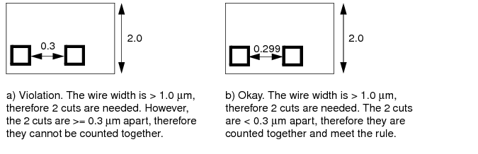
Specifies the number of cuts a via must have when it is on a wide wire or pin whose width is greater than width. The MINIMUMCUT rule applies to all vias touching this particular metal layer. You can specify more than one MINIMUMCUT rule per layer. (See Example 1-14.)
The MINIMUMCUT syntax is defined as follows:
[MINIMUMCUT numCuts WIDTH width
[WITHIN cutDistance]
[FROMABOVE | FROMBELOW]
[LENGTH length WITHIN distance]
;] ...
|
Specifies the number of cuts a via must have when it is on a wire or pin whose width is greater than width. |
||
|
WIDTH width |
Specifies the width of the wire or pin, in microns. |
|
|
WITHIN cutDistance |
||
|
Indicates that numCuts via cuts must be less than cutDistance from each other in order to be counted together to meet the minimum cut rule. (See Figure 1-12.) |
||
|
Indicates whether the rule applies only to connections from above this layer or from below. |
||
|
LENGTH length WITHIN distance |
||
|
Indicates that the rule applies for thin wires directly connected to wide wires, if the wide wire has a width that is greater than width and a length that is greater than length, and the vias on the thin wire are less than distance from the wide wire. (See Figure 1-11 ). The length value must be greater than or equal to the width value. If LENGTH and WITHIN are present, this rule only checks the thin wire connected to a wide wire, and does not check the wide wire itself. A separate MINIMUMCUT x WIDTH y ; statement without LENGTH and WITHIN is required for any wide wire minimum cut rule. |
||
Example 1-14 Minimum Cut Rules
The following MINIMUMCUT definitions show different ways to specify a MINIMUMCUT rule.
The following syntax specifies that two via cuts are required for metal4 wires that are greater than 0.5 μm when connecting from metal3 or metal5.
LAYER metal4
MINIMUMCUT 2 WIDTH 0.5 ;
The following syntax specifies that four via cuts are required for metal4 wires that are greater than 0.7 μm, when connecting from metal3.
LAYER metal4
MINIMUMCUT 4 WIDTH 0.7 FROMBELOW ;
The following syntax specifies that four via cuts are required for metal4 wires that are greater than 1.0 μm, when connecting from metal5.
LAYER metal4
MINIMUMCUT 4 WIDTH 1.0 FROMABOVE ;
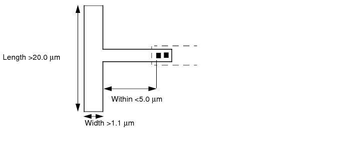
The following syntax specifies that two via cuts are required for metal4 wires that are greater than 1.1 μm wide and greater than 20.0 μm long, and the via cut is less than 5.0 μm from the wide wire. Figure 1-11 illustrates this example.
LAYER metal4
MINIMUMCUT 2 WIDTH 1.1 LENGTH 20.0 WITHIN 5.0 ;
Figure 1-11 Minimum Cut Rule
The following syntax specifies that two via cuts are required for metal4 wires that are greater than 1.0 μm wide. The via cuts must be less than 0.3 μm from each other in order to meet the minimum cut rule. Figure 1-12 illustrates this example.
MINIMUMCUT 2 WIDTH 1.0 WITHIN 0.3 ;
Figure 1-12 Minimum Cut Within Rule
MINIMUMDENSITY minDensity
Specifies the minimum metal density allowed for the layer, as a percentage. The minDensity and maxDensity values represent the metal density range within which all areas of the design must fall. The metal density must be greater than or equal to minDensity and less than or equal to maxDensity. For an example of this statement, see Example 1-12.
Type: Float
Value: Between 0.0 and 100.0
MINSIZE minWidth minLength [minWidth2 minLength2]
Specifies the minimum width and length of a rectangle that must be able to fit somewhere within each polygon on this layer (see Figure 1-13 ). All polygons must meet this MINSIZE rule, if no AREA rule is specified. If an AREA rule is specified, all polygons must meet either the MINSIZE or the AREA rule.
You can specify multiple rectangles by specifying a list of minWidth2 and minLength2 values. If more than one rectangle is specified, the MINSIZE rule is satisfied if any of the rectangles can fit within the polygon.
Type: Float, specified in microns, for all values
Example 1-15 Minimum Size and Area Rules
Assume the following minimum size and area rules:
TYPE ROUTING ;
AREA 0.07 ; #0.20 um x 0.35 um = 0.07 um^2
MINSIZE 0.14 0.30 ; #0.14 um x 0.30 um = 0.042 um^2
....
Figure 1-13 illustrates how these rules behave when one or both of the rules are present in the LAYER statement:
Figure 1-13 Minimum Size and Area Rules
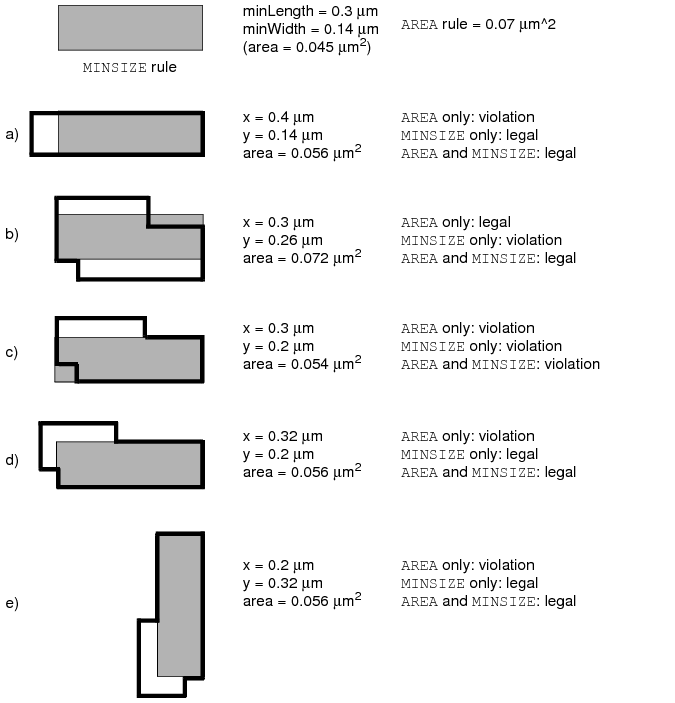
The following statement defines a MINSIZE rule that specifies that every polygon must have a minimum area of 0.07 μm2, or that a rectangle of 0.14 x 0.30 μm must be able to fit within the polygon, or that a rectangle of 0.16 x 0.26 μm must be able to fit within the polygon:
TYPE ROUTING ;
AREA 0.07 ; #0.20 x 0.35 um = 0.07 um^2
MINSIZE 0.14 0.30 0.16 0.26 ; #0.14 x 0.30 um = 0.042 um^2
#0.16 x 0.26 um = 0.0416 um^2
...
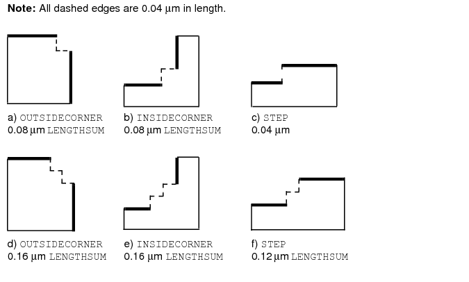
Specifies the minimum step size, or shortest edge length, for a shape. The MINSTEP rule ensures that Optical Pattern Correction (OPC) can be performed during mask creation for the shape.
Note: A single layer should only have one type of MINSTEP rule. It should include either INSIDECORNER, OUTSIDECORNER, or STEP statements (with an optional LENGTHSUM value), or one LENGTHSUM statement, or one MAXEDGES statement.
For an illustration of the MINSTEP rules, see Figure 1-14. For an example, see Example 1-16.
The syntax for MINSTEP is as follows:
[MINSTEP minStepLength
[ [INSIDECORNER | OUTSIDECORNER | STEP]
[LENGTHSUM maxLength]
| [MAXEDGES maxEdges] ;]
|
Specifies the minimum step size, or shortest edge length, for a shape. The edge of a shape must be greater than or equal to this value, or a violation occurs. |
||
|
Indicates that a violation occurs if two or more consecutive edges of an inside corner are less than minStepLength. If LENGTHSUM is also defined, a violation only occurs if the total length of all consecutive edges (that are less than minStepLength) is greater than maxLength. Shape b in Figure 1-14 shows an inside corner. It is considered an inside corner because the two edges >= minStepLength (shown with thick lines) that abut the consecutive short edges < minStepLength (shown with dashed lines) form an inside corner (or concave shape). |
||
|
Indicates that a violation occurs if two or more consecutive edges of an outside corner are less than minStepLength. If LENGTHSUM is also defined, a violation only occurs if the total length of all consecutive edges (that are less than minStepLength) is greater than maxLength. Shape a in Figure 1-14 shows an outside corner. It is considered an outside corner because the two edges >= minStepLength (shown with thick lines) that abut the consecutive short edges < minStepLength (shown with dashed lines) form an outside corner (or convex shape). Note: This is the default rule, if INSIDECORNER, OUTSIDECORNER, or STEP is not specified. |
||
|
Indicates that a violation occurs if one or more consecutive edges of a step are less than minStepLength. If LENGTHSUM is also defined, a violation only occurs if the total length of all consecutive edges (that are less than minStepLength) is greater than maxLength. Shape f in Figure 1-14 shows a step. It is considered a step because the two edges >= minStepLength (shown with thick lines) that abut the consecutive short edges < minStepLength (shown with dashed lines) form a step instead of a corner. |
||
|
LENGTHSUM maxLength |
||
|
Specifies the maximum total length of consecutive short edges (edges that are less than minStepLength) that OPC can correct without causing new DRC violations. If the total length of the edges is greater than maxLength, a violation occurs. No violation occurs if the total length is less than or equal to maxLength. |
||
|
MAXEDGES maxEdges |
||
|
Specifies that up to maxEdges consecutive edges that are less than minStepLength in length are allowed, but more than maxEdges in a row is a violation. Typically, most tools only allow a maxEdges value of 0, 1, or 2. A maxEdges value of 0 means that no edge can be less than minStepLength. Note: The maxEdges value of 1 will check the cases covered by OUTSIDECORNER and INSIDECORNER. However, there is no relationship between MAXEDGES and STEP. |
||
Example 1-16 Minimum Step Rules
|
|
The following table shows the results of the specified MINSTEP rules using the shapes in Figure 1-14. For these rules, assume minStepLength equals 0.05 μm, and that each dashed edge is 0.04 μm in length. |
|
OUTSIDECORNER is the default behavior. Therefore, shapes a and d are violations because their consecutive edges are less than 0.05 μm. Shapes b, c, e, and f are not outside corner checks. |
|
|
OUTSIDECORNER is the default behavior. Therefore, shapes a and d are checked and are legal because their consecutive edges are greater than or equal to 0.04 μm. |
|
|
Shape a is legal because its consecutive edges are less than 0.05 μm, and the total length of the edges is less than or equal to 0.08 μm. Shape d is a violation because even though its consecutive edges are less than 0.05 μm, the total length of the edges is greater than 0.08 μm. |
|
|
Shapes a and d are legal because the total length of their consecutive edges is less than or equal to 0.16 μm. |
|
|
Shapes b and e are violations because their consecutive edges are less than 0.05 μm. Shapes a, c, d, and f are not inside corner checks. |
|
|
Shape b is legal because its consecutive edges are less than 0.05 μm, and the total length of the edges is less than or equal to 0.15 μm. Shape e is a violation because even though its consecutive edges are less than 0.05 μm, the total length of the edges is greater than 0.15 μm. |
|
|
Shapes c and f are violations because their consecutive edges are less than 0.05 μm. Shapes a, b, d, and e are not step checks. |
|
|
Shape c is legal because its consecutive edges are less than 0.05 μm, and the total length of the edges is less than or equal to 0.08 μm. Shape f is a violation because even though its consecutive edges are less than 0.05 μm, the total length of the edges is greater than 0.08 μm. |
|
|
Shapes c and f are legal because their consecutive edges are greater than or equal to 0.04 μm. |
|
|
Figure 1-15 shows the results of the following MINSTEP MAXEDGES rule: |
MINSTEP 1.0 MAXEDGES 2 ;
Figure 1-15
MINWIDTH width
Specifies the minimum legal object width on the routing layer. For example, MINWIDTH 0.15 specifies that the width of every object must be greater than or equal to 0.15 μm. This value is used for verification purposes, and does not affect the routing width. The WIDTH statement defines the default routing width on the layer.
Default: The value of the WIDTH statement
Type: Float, specified in microns
OFFSET {distance | xDistance yDistance}
Specifies the offset for the routing grid from the design origin for the layer. This value is used to align routing tracks with standard cell boundaries, which helps routers get good on-grid access to the cell pin shapes. For best routing results, most standard cells have a 1/2 pitch offset between the MACRO SIZE boundary and the center of cell pins that should be aligned with the routing grid. Normally, it is best to not set the OFFSET value, so the software can analyze the library to determine the best offset values to use, but in some cases it is necessary to force a specific offset.
Generally, it is best for all of the horizontal layers to have the same offset and all of the vertical layers to have the same offset, so that routing grids on different layers align with each other. Higher layers can have a larger pitch, but for best results, they should still align with a lower layer routing grid every few tracks to make stacked-vias more efficient.
Default: The software is allowed to determine its own offset values for preferred and non-preferred routing tracks.
Type: Float, specified in microns
|
Specifies the offset value that is used for the preferred direction routing tracks. |
||
|
Specifies the x offset for vertical routing tracks, and the y offset for horizontal routing tracks. |
||
PITCH {distance | xDistance yDistance}
Specifies the required routing pitch for the layer. Pitch is used to generate the routing grid (the DEF TRACKS). For more information, see "Routing Pitch".
Type: Float, specified in microns
|
Specifies one pitch value that is used for both the x and y pitch. |
||
PROPERTY propName propVal
Specifies a numerical or string value for a layer property defined in the PROPERTYDEFINITIONS statement. The propName you specify must match the propName listed in the PROPERTYDEFINITIONS statement.
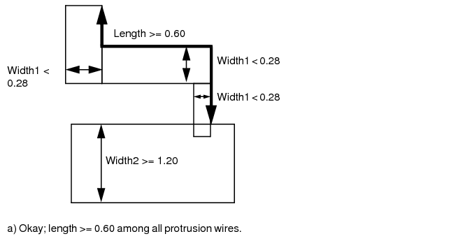
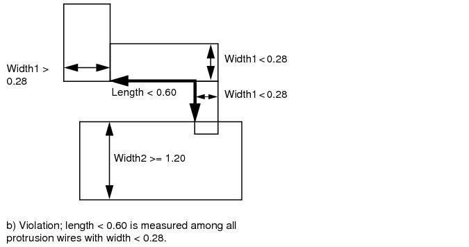
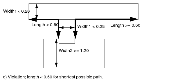
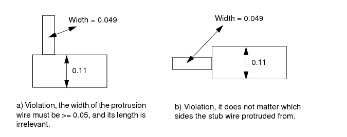
PROTRUSIONWIDTH width1 LENGTH length WIDTH width2
Specifies that the width of a protrusion must be greater than or equal to width1 if it is shorter than length, and it connects to a wire that has a width greater than or equal to width2 (see Figure 1-16 ). Length is determined by the shortest possible path among all of the protrusion wires with width smaller width1, and is measured by the shortest outside edges of the wires.
Type: Float, specified in microns
Example 1-17 Protrusion
The following example specifies that a protrusion must have a width that is greater than or equal to 0.28 μm, if the length of the protrusion is less than 0.60 μm and the wire it connects to has a width that is greater than or equal to 1.20 μm.
...
PROTRUSIONWIDTH 0.28 LENGTH 0.60 WIDTH 1.20 ;
...
If the given value of LENGTH in PROTRUSIONWIDTH is zero, then the length of the protrusion wire is irrelevant. In this case, the width of the protrusion wire should always be checked independent of the length of the wire. The following example illustrates this rule:
PROTRUSIONWIDTH 0.05 LENGTH 0 WIDTH 0.11 ; " ;
RESISTANCE RPERSQ value
Specifies the resistance for a square of wire, in ohms per square. The resistance of a wire can be defined as
|
RPERSQU x wire length/wire width |
SHRINKAGE distance
Specifies the value to account for shrinkage of interconnect wiring due to the etching process. Actual wire widths are determined by subtracting this constant value.
Type: Float
Specifies the spacing rules to use for wiring on the layer. You can specify more than one spacing rule for a layer. See "Using Spacing Rules".
The syntax for describing spacing rules is defined as follows:
[SPACING minSpacing
[ RANGE minWidth maxWidth
[ USELENGTHTHRESHOLD
| INFLUENCE influenceLength
[RANGE stubMinWidth stubMaxWidth]
| RANGE minWidth maxWidth]
| LENGTHTHRESHOLD maxLength
[RANGE minWidth maxWidth]
| ENDOFLINE eolWidth WITHIN eolWithin
[PARALLELEDGE parSpace WITHIN parWithin
[TWOEDGES]]
| SAMENET [PGONLY]
| NOTCHLENGTH minNotchLength
| ENDOFNOTCHWIDTH endOfNotchWidth
NOTCHSPACING minNotchSpacing
NOTCHLENGTH minNotchLength
]
;] ...
|
SPACING minSpacing |
||
|
Specifies the default minimum spacing, in microns, allowed between two geometries on different nets. |
||
|
RANGE minWidth maxWidth |
||
|
Indicates that the minimum spacing rule applies to objects on the layer with widths in the indicated RANGE (that is, widths that are greater than or equal to minWidth and less than or equal to maxWidth). If you do not specify a range, the rule applies to all objects. Note: If you specify multiple RANGE rules, the range values should not overlap. |
||
|
Indicates that the threshold spacing rule should be used if the other object meets the previous LENGTHTHRESHOLD value. |
||
|
INFLUENCE influenceLength |
||
|
Indicates that any length of the stub wire that is less than or equal to influenceLength from the wide wire inherits the wide wire spacing. The influence rule applies to stub wires on the layer with widths in the indicated RANGE (that is, widths that are greater than or equal to stubMinWidth and less than or equal to stubMaxWidth). If you do not specify a range, the rule applies to all stub wires. Note: Specifying the INFLUENCE keyword denotes that the statement only checks the influence rule, and does not check normal spacing. You must also specify a separate SPACING statement for normal spacing checks. |
||
|
RANGE minWidth maxWidth |
||
|
Specifies an optional second width range. The spacing rule applies if the widths of both objects fall in the ranges defined (each object in a different range). For an object's width to fall in a range, it must be greater than or equal to minWidth and less than or equal to maxWidth. Note: If you specify multiple RANGE rules, the range values should not overlap. |
||
|
LENGTHTHRESHOLD maxLength |
||
|
Specifies the maximum parallel run length or projected length with an adjacent metal object for this spacing value. The minSpacing value should be less than or equal to the "default" minSpacing value when no LENGTHTHRESHOLD is specified for this range of widths. For an example, see "Using Spacing Rules". The threshold spacing rule applies to objects with widths in the indicated RANGE (that is, widths that are greater than or equal to minWidth and less than or equal to maxWidth). If you do not specify a range, the rule applies to all objects. Note: If you specify multiple RANGE rules, the range values should not overlap. |
||
|
ENDOFLINE eolWidth WITHIN eolWithin |
||
|
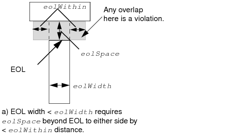
Indicates that an edge that is shorter than eolWidth, noted as end-of-line (EOL from now on) edge requires spacing greater than or equal to eolSpace beyond the EOL anywhere within (that is, less than) eolWithin distance (see Figure 1-17 ). Typically, eolSpace is slightly larger than the minimum allowed spacing on the layer. The eolWithin value must be less than the minimum allowed spacing. |
||
|
|
||
|
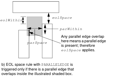
PARALLELEDGE parSpace WITHIN parWithin |
||
|
Indicates the EOL rule applies only if there is a parallel edge that is less than parSpace away, and is also less than parWithin from the EOL and eolWithin beyond the EOL (see Figure 1-18 ). |
||
|
|
||
|
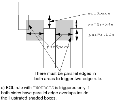
If TWOEDGES is specified, the EOL rule applies only if there are two parallel edges that meet the PARALLELEDGE parSpace, eolWithin, and parWithin parameters (see Figure 1-19 ). |
||
|
|
||
|
Indicates that the minSpacing value only applies to same-net metal. If PGONLY also is specified, the minSpacing value only applies to same-net metal that is a power or ground net. This rule typically is used when a technology has wider spacing for wider width wires; however, it still allows minimum spacing for same-net wires, even if they are wide. (See Example 1-19.) |
||
|
NOTCHLENGTH minNotchLength |
||
|
Indicates that any notch with a notch length less than minNotchLength must have notch spacing greater than or equal to minSpacing. (See illustration a in Figure 1-26.) The value you specify for minSpacing should be only slightly larger than the normal minimum spacing rule (typically, between 1x and 1.5x minimum spacing). Note: You can specify only one NOTCHLENGTH rule per layer. |
||
|
ENDOFNOTCHWIDTH endOfNotchWidth |
||
|
Indicates that the notch metal at the bottom end of a U-shaped notch requires spacing that is greater than or equal to minSpacing, if the notch has a width that is less than endOfNotchWidth, notch spacing that is less than or equal to minNotchSpacing, and notch length that is greater than or equal to minNotchLength. The spacing is required for the extent of the notch. The values you specify for notchSpacing and minSpacing should be only slightly larger than the normal minimum spacing rule (typically between 1x and 1.5x minimum spacing). The value you specify for endOfNotchWidth should be only slightly larger than the minimum width rule (typically, between 1x and 1.5x minimum width). Note: You can specify only one ENDOFNOTCHWIDTH rule per layer. |
||
When defined with a RANGE argument, a spacing value applies to all objects with widths within a specified range. That is, the rule applies to objects whose widths are greater than or equal to the specified minimum width and less than or equal to the specified maximum width.
Note: If you specify multiple RANGE arguments, the RANGE values should not overlap.
In the following example, the default minimum allowed spacing between two adjacent objects is 0.3 μm. However, for objects between 0.5 and 1.0 μm in width, the spacing is 0.4 μm. For objects between 1.01 and 2.0 μm in width, the spacing is 0.5 μm.
SPACING 0.5 RANGE 1.01 2.0 ; #The RANGE begins at 1.01 and not 1.0 because
#RANGE values should not overlap.
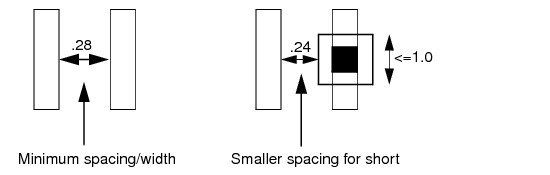
In the following example, a slightly tighter spacing of .24 μm is needed if the other object is less than or equal to 1.0 μm in length (see Figure 1-20 ).
SPACING 0.24 LENGTHTHRESHOLD 1.0 ;
The USELENGTHTHRESHOLD argument specifies that the threshold spacing rule should be applied if the other object meets the previous LENGTHTHRESHOLD value.
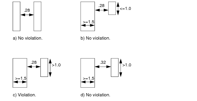
In the following example, a larger spacing of 0.32 μm is needed for wire widths between 1.5 and 9.99 μm. However, if the other object is less than or equal to 1.0 μm in length, the smaller .0.28 μm spacing is applied (see Figure 1-21 ).
SPACING 0.28 ; #Default minimum spacing is >=0.28 um.
SPACING 0.28 LENGTHTHRESHOLD 1.0 ; #For short parallel lengths of <= 1.0 um,
SPACING 0.32 RANGE 1.5 9.99 USELENGTHTHRESHOLD ;
#Wide wires with 1.5 <= width <=9.99 need
#0.32 spacing unless the parallel run
#length is <= 1.0 from the previous rule.
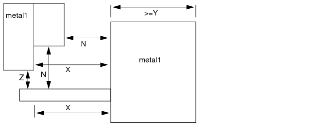
In Figure 1-22 , a minimum space of N is required between two metal lines when at least one metal line has a width that is >= Y. This spacing must be maintained for any small piece of metal (<Y) that is connected to the wide metal within X range of the wide metal. Outside of this range, normal spacing rules (Z) apply.
In the following example, the 0.5 μm spacing applies for the first 1.0 μm of the stub sticking out from the large object. This rule only applies to the stub wire; the previous rule must be included for the wide wire spacing. The SPACING 0.5 RANGE 2.01 2000.0 statement is required to get extra spacing for the wide-wire itself.
SPACING 0.5 RANGE 2.01 2000.0 ;
SPACING 0.28 ; #Minimum spacing is >= 0.28 um.
SPACING 0.5 RANGE 2.01 2000.0 ; #wide-wire >= 2.01 um wide requires 0.5um spacing
SPACING 0.5 RANGE 2.01 2000.0 INFLUENCE 1.000 ;
#Stub wires <= 1.0 um from wide wires >= 2.01
Some processes only need the INFLUENCE rule for certain widths of the stub wire. In the following example, the 0.5 μm spacing is required only for stub wires between 0.5 and 1.0 μm in width.
SPACING 0.28 ; #Minimum spacing is >= 0.28 um.
SPACING 0.5 RANGE 2.01 2000.0 ; #wide-wire >= 2.01 um wide requires 0.5um spacing
SPACING 0.5 RANGE 2.01 2000.0 INFLUENCE 1.00 RANGE 0.5 1.0 ;
#Stub wires with 0.5 <= width <= 1.0, and <= 1.0 um from
#wide wide wires >= 2.01 require 0.5 um spacing.
Example 1-18 EOL Spacing Rules
SPACING 1.0 ; #minimum spacing is 1.0 μm
SPACING 1.2 ENDOFLINE 1.3 WITHIN 0.6 ;
Any EOL that is less than 1.3 μm wide requires spacing that is greater than or equal to 1.2 μm beyond the EOL, within 0.6 μm to either side. Figure 1-23 includes examples of legal spacing for, and violations of, this rule.
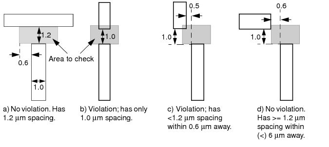
SPACING 1.0 ; #minimum spacing is 1.0 μm
SPACING 1.2 ENDOFLINE 1.3 WITHIN 0.6 PARALLELEDGE 1.1 WITHIN 0.5 ;
Any line that is less than 1.3 μm wide, with a parallel edge that is less than 1.1 μm away, and is within 0.5 μm of the EOL, requires spacing greater than or equal to 1.2 μm beyond the EOL, within 0.6 μm to either side of the EOL. Figure 1-24 includes examples of legal spacing for, and violations of, this rule.
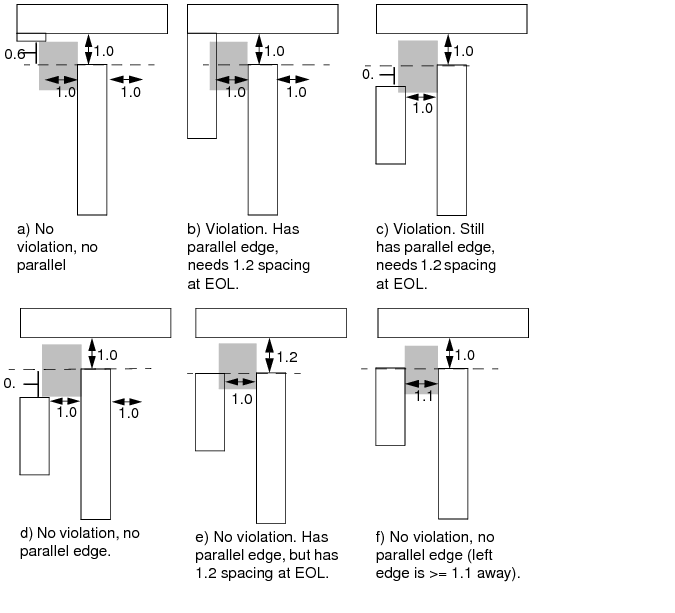
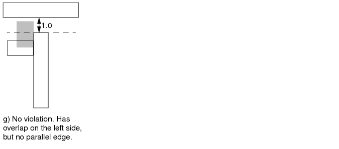
SPACING 1.0 ; #minimum spacing is 1.0 μm
SPACING 1.2 ENDOFLINE 1.3 WITHIN 0.6 PARALLELEDGE 1.1 WITHIN 0.5 TWOEDGES ;
Example 1-19 Same Net Spacing Rule
If you include the following routing layer rules in your LEF file, same-net power or ground nets can use 1.0 μm spacing, even if they are 2 μm to 5 μm wide, as shown in Figure 1-25 :
LAYER M1
TYPE ROUTING ;
SPACING 1.0 ; #min spacing is 1.0
SPACING 1.5 RANGE 2.0 5.0 ; #need 1.5 spacing for 2 to 5 μm wide wires
SPACING 1.0 SAMENET PGONLY ;
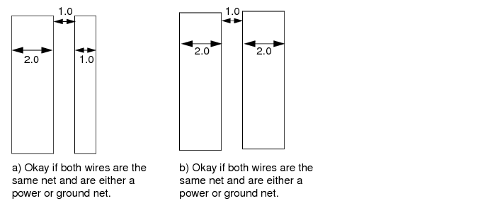
Example 1-20 Notch Length Spacing Rule
The figure below illustrates the following routing layer rules:
SPACING 0.12 NOTCHLENGTH 0.15 ;
Figure 1-26 Notch Length Rule Definitions
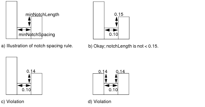
Example 1-21 End Of Notch Width Spacing Rule
If you include the following routing layer rules in your LEF file, the notch metal at the bottom end of a U-shaped notch must have spacing that is greater than or equal to 0.14 μm, if the notch metal has a width that is less than 0.15 μm, notch spacing that is less than or equal to 0.16 μm, and notch length that is greater than or equal to 0.08 μm. See Figure 1-27 for different layout examples for these rules.
SPACING 0.10 ; #default spacing
SPACING 0.14 ENDOFNOTCHWIDTH 0.15 NOTCHSPACING 0.16 NOTCHLENGTH 0.08 ;
Figure 1-27 End Of Notch Width Rule Definitions
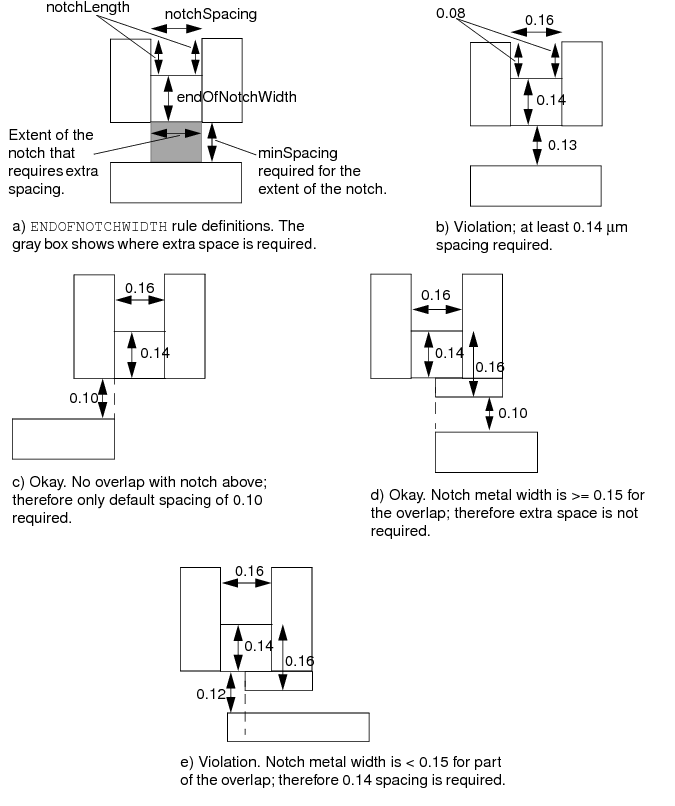
Specifies the spacing tables to use for wiring on the layer. You can specify only one parallel run length and one influence spacing table for a layer. For information on and examples of using spacing tables, see "Using Spacing Tables".
The syntax for describing spacing tables is defined as follows:
[SPACINGTABLE
PARALLELRUNLENGTH {length} ...
{WIDTH width {spacing} ...}... ;
[SPACINGTABLE
INFLUENCE {WIDTH width WITHIN distance
SPACING spacing} ... ;]
| TWOWIDTHS {WIDTH width [PRL runLength]
{spacing} ...} ... ;
;]
|
PARALLELRUNLENGTH {length} ... |
||
|
Specifies the maximum parallel run length between two objects, in microns. If the maximum width of the two objects is greater than width, and the parallel run length is greater than length, then the spacing between the objects must be greater than or equal to spacing. The first spacing value is the minimum spacing for a given width, even if the PRL value is not met. You must specify length, width, and spacing values in increasing order. |
||
|
TWOWIDTHS {WIDTH width [PRL runLength] {spacing} ...} |
||
|
Creates a table in which the spacing between two objects depends on the widths of both objects (instead of just the widest width). Optionally, it also can depend on the parallel run length between the two objects (PRL). For more information, see "Two-Width Spacing Tables." The first width value should be 0 without an accompanied run length definition. The PRL values in SPACINGTABLE TWOWIDTHS statement can be negative, which should be interpreted in the same way as in SPACINGTABLE PARLLELRUNLENGTH rules. |
||
|
INFLUENCE {WIDTH width WITHIN distance SPACING spacing ...} |
||
|
Creates a table that enforces wide wire spacing rules between nearby perpendicular wires. If an object has a width that is greater than width, and is located less than distance from two perpendicular wires, then the spacing between the perpendicular wires must be greater than or equal to spacing. You must specify width values in increasing order. Note: You can only specify an INFLUENCE table if you specify a PARALLELRUNLENGTH table first. |
||
You can specify some of the SPACING statements with the SPACINGTABLE statements. For example, the following SPACING statements can be specified with SPACINGTABLE:
SPACING x SAMENET ___ ;
SPACING x ENDOFLINE ___ ;
SPACING x NOTCHLENGTH ___ ;
SPACING x ENDOFNOTCHWIDTH ___ ;
These SPACING checks are orthogonal to the SPACINGTABLE checks, except SAMENET spacing will override SPACINGTABLE for same-net objects.
However, you cannot specify some SPACING statements (as given below) with SPACINGTABLE as these would generate semantic errors.
SPACING x ;
SPACING x RANGE ___ ;
SPACING x LENGTHTHRESHOLD ___ ;
Some processes have complex width and length threshold rules. Instead of creating multiple SPACING rules with different LENGTHTHRESHOLD and RANGE statements, you can define the information in a spacing table.
For example, for Figure 1-28 , a typical 90nm DRC manual might have the following rules described:
|
0.15 μm spacing |
|
|
Either width>0.25 μm and parallel length>0.50 μm |
0.20 μm spacing |
|
Either width>1.50 μm and parallel length>0.50 μm |
0.50 μm spacing |
|
Either width>3.00 μm and parallel length>3.00 μm |
1.00 μm spacing |
|
Either width>5.00 μm and parallel length>5.00 μm |
2.00 μm spacing |
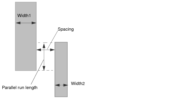
These rules translate into the following SPACINGTABLE PARALLELRUNLENGTH statement:
...
SPACINGTABLE
PARALLELRUNLENGTH 0.00 0.50 3.00 5.00 #lengths must be increasing
WIDTH 0.00 0.15 0.15 0.15 0.15 #max width>0.00
WIDTH 0.25 0.15 0.20 0.20 0.20 #max width>0.25
WIDTH 1.50 0.15 0.50 0.50 0.50 #max width>1.50
WIDTH 3.00 0.15 0.50 1.00 1.00 #max width>3.00
WIDTH 5.00 0.15 0.50 1.00 2.00 ; #max width>5.00
...
Using the SPACINGTABLE PARALLELRUNLENGTH statement, the rules can be described in the following way:
Processes often require a second spacing table to enforce the wide wire spacing rules between nearby perpendicular wires, even if the wires are narrow. Figure 1-29 illustrates this situation. Use the following SPACINGTABLE INFLUENCE syntax to describe this table:
If a wire has a width that is greater than width, and the distance between it and two other wires is less than distance, the other wires must be separated by spacing that is greater than or equal to spacing. Typically, the distance and spacing values are the same. Note that the distance halo extends horizontally, but not into the corners.
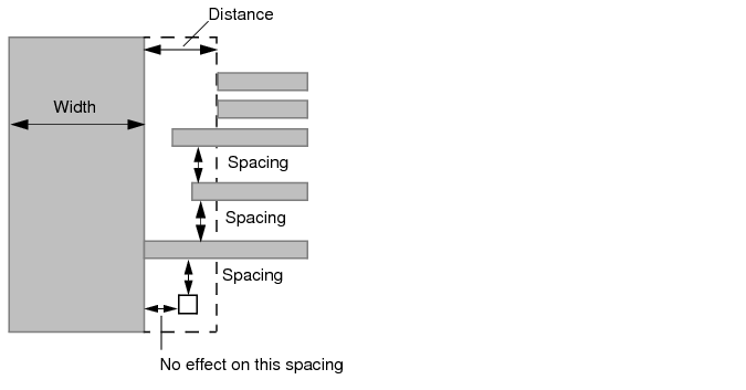
The wide wire rules often match the larger width and spacing values in the SPACINGTABLE PARALLELRUNLENGTH values. The previously described rules translate into the following SPACINGTABLE INFLUENCE statement:
...
SPACINGTABLE INFLUENCE
WIDTH 1.50 WITHIN 0.50 SPACING 0.50 #w>1.50, dist<0.50, needs sp>=0.50
WIDTH 3.00 WITHIN 1.00 SPACING 1.00 #widths must be increasing
WIDTH 5.00 WITHIN 2.00 SPACING 2.00 ;
...
You can create a table that enforces spacing rules that depends on the width of both objects instead of just the widest width, and optionally depends on the parallel run length between the two objects. You can use this table to replace existing SPACING ...RANGE...RANGE rules to make it easier to read, and to include parallel run length effects in one common table. Use the following SPACINGTABLE TWOWIDTHS syntax to describe this table:
To find the required spacing, a 2-dimensional table is used that implicitly has the same widths (and optional parallel run lengths) for the row and column headings. There must be exactly as many spacing values in each WIDTH row as there are WIDTH rows. The width and runLength values must be the same or increasing from top to bottom in the table. The spacing values must be the same or increasing from left to right, and from top to bottom in the table.
Given two objects with width1, width2, and a parallel overlap of runLength, you find the spacing using the following method:
|
|
Find the last row where both width1 is greater than the table row width, and runLength is greater than the table row run length. If no table row run length exists, the runLength value is not checked for that row (only that width1 is greater than table row width is checked). |
|
|
Find the right-most column where both width2 is greater than table column width and runLength is greater than table column run length. If no table column run length exists, the runLength value is not checked for that column (only that width2 is greater than table column width is checked). |
For example, assume a DRC manual has the following rules described:
|
0.15 μm spacing |
|
|
Either width>0.25 μm and parallel length>0.0 μm |
0.20 μm spacing |
|
Both width>0.25 μm and parallel length>0.0 μm |
0.25 μm spacing |
|
Either width>1.50 μm and parallel length>1.50 μm |
0.50 μm spacing |
|
Both width>1.50 μm and parallel length>1.50 μm |
0.60 μm spacing |
|
Either width>3.00 μm and parallel length>3.00 μm |
1.00 μm spacing |
|
Both width>3.00 μm and parallel length>3.00 μm |
1.20 μm spacing |
The rules translate into the following SPACINGTABLE:
WIDTH 0.00 0.15 0.20 0.50 1.00
WIDTH 0.25 PRL 0.0 0.20 0.25 0.50 1.00
WIDTH 1.50 PRL 1.50 0.50 0.50 0.60 1.00
WIDTH 3.00 PRL 3.00 1.00 1.00 1.00 1.20 ;
Note that both width and parallel run length (if specified) must be exceeded to index into the row and column. Therefore, in this example:
THICKNESS distance
Specifies the thickness of the interconnect.
Type: Float
Identifies the layer as a routable layer.
WIDTH defaultWidth
Specifies the default routing width to use for all regular wiring on the layer.
Type: Float
WIREEXTENSION value
Specifies the distance by which wires are extended at vias. You must specify a value that is more than half of the routing width.
Default: Wires are extended half of the routing width
Type: Float
Note: The WIREEXTENSION statement only extends wires and not vias. For 65nm and below, WIREEXTENSION is no longer recommended because it may generate some advance rule violations if wires and vias have different widths.
The following figure shows WIREEXTENSION with same and different wire and via widths:
Figure 1-30 Illustration of WIREEXTENSION
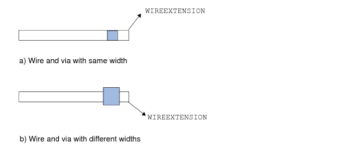
A type rule can be used to further classify a routing layer.
You can create a type rule by using the following property definition:
You can create a span length table rule by using the following property definition:
|
ORTHOGONAL length |
Specifies that the length between two inside facing corners of a rectilinear object must be greater than or equal to the length. Type: Float, specified in microns |
|
EXCEPTOTHERSPAN otherSpanlength |
|
|
Indicates that the span length rule only applies if the span length on the perpendicular direction is greater than the specified otherSpanlength. This construct must be defined on a layer with RECTONLY. Otherwise, the span length in the orthogonal direction could be ambiguous in a polygon shape. |
|
|
SPANLENGTHTABLE {spanLength)}... |
|
|
Specifies all of the allowable legal span lengths on the routing layer. All of the given span lengths are exact values, except for the last one, which is greater than equal to the value. All of the possible span lengths of an object in both directions should be checked against the given span length values. At most, two SPANLENGTHTABLE spacing tables can be defined - one with WRONGDIRECTION and the other without. |
|
|
Specifies all of the allowable legal span lengths in the direction parallel to the specified direction in DIRECTION on a Manhattan routing layer. Note that using WRONGDIRECTION changes the interpretation of any wrong-way routing widths in the DEF NETS section. If WRONGDIRECTION is specified, then any wrong-way routing in the DEF NETS section will use the WRONGDIRECTION width for that layer unless the net or route has a NONDEFAULTRULE with a WIDTH greater than the WRONGDIRECTION width. But, the implicit default route-extension is still half of the preferred direction width. |
|
Span Length Table Rule Examples
|
|
The following example is an illustration of SPANLENGTHTABLE {spanLength}… ORTHOGONAL length and SPANLENGTHTABLE {spanLength}… WRONGDIRECTION with preferred direction being horizontal: |
Figure 1-31 Illustration of SPANLENGTHTABLE
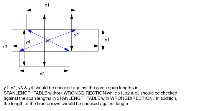
You can use width table rules to define all the allowable legal widths on the routing layer.
You can define a width table rule by using the following property definition:
|
Specifies that one of the right or wrong direction width between two inside corners of a rectilinear object must be greater than or equal to the first width value in the WIDTHTABLE in the corresponding direction, if WIDTHTABLE WRONGDIRECTION is specified. Otherwise, the width between the corners must be greater than or equal to the first width value in the WIDTHTABLE (for both directions) either vertically or horizontally. |
|
|
WIDTHTABLE {width}... |
|
|
The WIDTH syntax should be used to define the default routing width on the layer, which should match one of the values in the WIDTHTABLE statement. In case that the last value of WIDTHTABLE denotes the exact width also, the MAXWIDTH statement with the last value can be used to represent it. At the most, two WIDTHTABLE spacing tables can be defined, one with WRONGDIRECTION and the other without it. Type: Float, specified in microns. |
|
|
Specifies that the allowable legal widths are for wires with direction perpendicular to the specified direction in DIRECTION on a Manhattan routing layer. Note that using WRONGDIRECTION changes the interpretation of any wrong-way routing widths in the DEF NETS section. If WRONGDIRECTION is specified, then any wrong-way routing in the DEF NETS section will use the WRONGDIRECTION width for that layer unless the net or route has a NONDEFAULTRULE with a WIDTH greater than the WRONGDIRECTION width. But, the implicit default route-extension is still half of the preferred direction width. |
|
|
|
The following width table rule indicates that width must be 0.10 μm, 0.15 μm, 0.20 μm, 0.25 μm, 0.30 μm, and greater than or equal to 0.40 μm. |
MAXWIDTH 0.40 ; # To define legal width =, instead of >=, 0.40 μm.
PROPERTY LEF58_WIDTHTABLE
"WIDTHTABLE 0.10 0.15 0.20 0.25 0.30 0.40 ;" ;
Figure 1-32 Illustration of WIDTHTABLE Rule
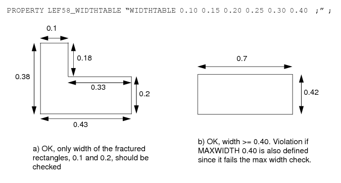
DIRECTION VERTICAL ;
PROPERTY LEF58_WIDTHTABLE
"WIDTHTABLE 0.05 0.1 0.15 WRONGDIRECTION ; " ;
Figure 1-33 Illustration of Width Table Rule with ORTHOGONAL and WRONGDIRECTION
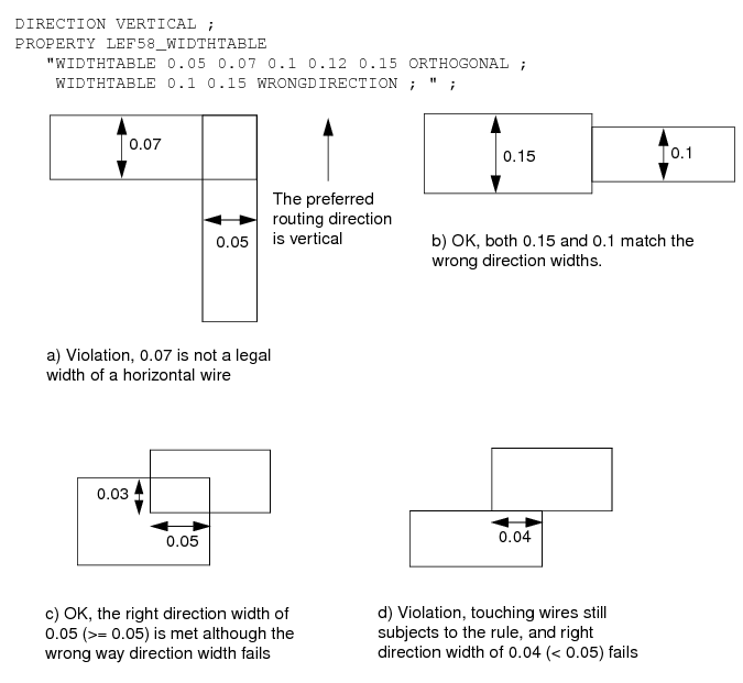
You can define a width rule by using the following property definition:
WIDTH is the same as the existing routing layer WIDTH syntax.
|
Specifies the default routing width to use for all regular wiring with direction perpendicular to the specified direction in DIRECTION on a Manhattan routing layer. Note that using WRONGDIRECTION changes the interpretation of any wrong-way routing widths in the DEF NETS section. If WRONGDIRECTION is specified, then any wrong-way routing in the DEF NETS section will use the WRONGDIRECTION width for that layer unless the net or route has a NONDEFAULTRULE with a WIDTH greater than the WRONGDIRECTION width. But, the implicit default route-extension is still half of the preferred direction width. |
|
|
The following width rule indicates that the default routing width of a vertical route is 0.1 μm, while the default routing width of a horizontal route is 0.14 μm: |
DIRECTION VERITICAL;
WIDTH 0.1;
PROPERTY LEF58_WIDTH
"WIDTH 0.14 WRONGDIRECTION ;" ;
In the DEF, a vertical default route in the NETS section will have a width of 0.10 μm with extension of 0.05 μm, while a horizontal route will have a width of 0.14 μm with extension of 0.05 μm.
In more advanced nodes, wider widths are required for non-preferred direction. The following example shows route with wrong-way segment:
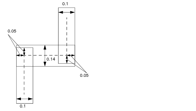
Figure 1-34 Illustration of WIDTH Rule with WRONGDIRECTION
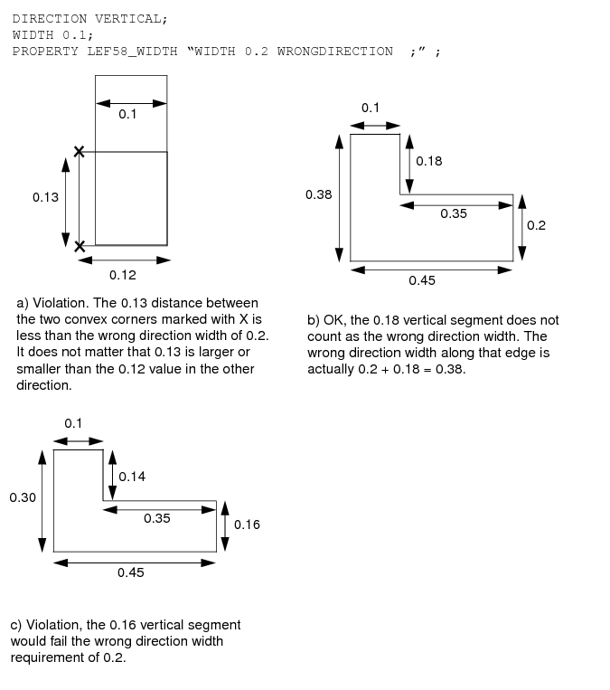
The PITCH statements define the detail routing grid generated when you initialize a floorplan. The pitch for a given routing layer defines the distance between routing tracks in the preferred direction for that layer. The complete routing grid is the union of the tracks generated for each routing layer.
You can include libraray properties in your LEF file to create 32/28 nm and smaller nodes rules that currently are not supported by existing LEF syntax. The properties are specified inside the PROPERTYDEFINITIONS statements.
All properties use the following syntax within the LEF PROPERTYDEFINITIONS statement:
The property definitions for the library properties are as follows:
LIBRARY LEF58_OALAYERMAP STRING ;
You can define an OpenAccess layer map rule by using the following PROPERTYDEFINITIONS statement:
PROPERTYDEFINITIONS
LIBRARY LEF58_OALAYERMAP STRING
"OALAYERMAP oaLayer
LAYER layer [MASK maskNum]
;..." ;
END PROPERTYDEFINITIONS
|
OALAYERMAP oaLayer LAYER layer [MASK maskNum] |
|
|
Specifies the equivalent OpenAccess layer name oaLayer of LEF layer layer. If MASK is specified only on a multi-patterning layer with MASK, only maskNum shapes would be mapped to the given OpenAcess layer name. If MASK is specified, there would be multiple such properties for each of the possible masks. |
|
OpenAccess Layer Map Rule Examples
|
|
The following example indicates that the LEF layer M1 is mapped to OpenAccess layer Metal1: |
PROPERTYDEFINITIONS
LIBRARY LEF58_OALAYERMAP STRING "
OALAYERMAP Metal1 LAYER M1 ; " ;
END PROPERTYDEFINITIONS
|
|
The following example indicates that the LEF MASK 1 shapes on M1 would go to OpenAccess layer Metal1A while MASK 2 shapes on M1 would go to OpenAccess layer Metal1B: |
PROPERTYDEFINITIONS
LIBRARY LEF58_OALAYERMAP STRING "
OALAYERMAP Metal1A LAYER M1 MASK 1 ;
OALAYERMAP Metal1B LAYER M1 MASK 2 ; " ;
END PROPERTYDEFINITIONS
Note: The keywords must be specified in the given order. For example if ORIGIN and SITE are both defined, ORIGIN must be specified first.
Specifies the macro type. If you do not specify CLASS, the macro is considered a CORE macro, and a warning prints when the LEF file is read in. You can specify macros of the following types:
|
Macro with data that is fixed to the floorplan and cannot change, such as power routing (ring pins) around the core. The placers understand that CLASS COVER cells have no active devices (such as diffusion or polysilicon), so the MACRO SIZE statement does not affect the placers, and you do not need an artificial OVERLAP layer. However, any pin or obstruction geometry in the COVER cells can affect the pin access checks done by the placers. A cover macro can be of the following sub-class: BUMP--A physical-only cell that has bump geometries and pins. Typically a bump cell has geometries only on the top-most "bump" metal layer, although it might contain a via and pin to the metal layer below. |
||
|
Large macro that has an internal power mesh, and only exposes power-pin shapes that form a ring along the macro boundary. When power stripes are added across the macro, they connect to each side of the ring-pin but do not go inside the ring. The CLASS RING macro can also be used for power-switch cells that are abutted together to form a power-ring around a power-domain. In that case, their power-pins have the same effect of interrupting power stripes as the ring-pins in a single block RING macro. |
||
|
Predefined macro used in hierarchical design. A block macro can have one of the following sub-classes: BLACKBOX--A block that sometimes only contains a SIZE statement that estimates its total area. A blackbox can optionally contain pins, but in many cases, the pin names are taken from a Verilog description and do not need to match the LEF MACRO pin names. SOFT--A cell that also contains a version of the sub-block that is not fully implemented. Normally, a soft block LEF can still have certain parts of it modified (for example, the aspect ratio, or pin locations) because the sub-block is not yet fully implemented. Any changes should be passed to the sub-block implementation. In contrast, a BLACKBOX has no sub-block implementation available. |
||
|
I/O pad. A pad can be one of the following types: INPUT, OUTPUT, INOUT, POWER, or SPACER, for I/O rows; INPUT, OUTPUT, INOUT, or POWER, for I/O corner pads; AREAIO for area I/O driver cells that do not have the bump built in as part of the macro (and therefore require routing to a CLASS COVER BUMP macro for a connection to the IC package). |
||
|
A standard cell used in the core area. CORE macros should always contain a SITE definition so that standard cell placers can correctly align the CORE macro to the standard cell rows. A core macro can be one of the following types: FEEDTHRU--Used for connecting to another cell. TIEHIGH,TIELOW--Used for connecting unused I/O terminals to the power or ground bus. The software does not rely on this sub-class. A tie-cell has to be CLASS CORE, but the software does not consider the sub-class to determine its type. The dotlib representation of the cell's output pin is considered, and based on the function on that pin, it is determined whether it is a tiehigh, or tielow. SPACER--Sometimes called a filler cell, this cell is used to fill in space between regular core cells. The SPACER sub-class needs to be cells with no logic-pins. Thus even with the sub-class defined, a cell will not be considered SPACER (also called FILLER) unless it has no logic/signal pins. A filler can only have Power and Ground pins. The instances of these cells will be marked by the insertion command to be of type 'Physical'. ANTENNACELL--Used for solving process antenna violations. This cell has a single input to a diode to bleed off charge that builds up during manufacturing. WELLTAP--Standard cell that connects N and P diffusion wells to the correct power or ground wire. The WELLTAP cells provide a tap for the N and P wells to the power/ground wires. |
||
|
A macro placed at the ends of core rows (to connect with power wiring). If the library includes only one corner I/O macro, then appropriate SYMMETRY must be included in its macro description. An ENDCAP macro can be one of the following types: The ENDCAP sub-class is required. The PRE and POST are CORE area cells, whereas the other four are PAD CLASS. |
Example 1-22 Macro Pad Cell
CLASS PAD ;
FOREIGN PAD_0 0.000 0.000 ;
ORIGIN 0.000 0.000 ;
SIZE 100.000 BY 300.000 ;
SYMMETRY X Y R90 ;
SITE PAD_SITE ;
PIN VDD
DIRECTION INOUT ;
USE POWER ;
SHAPE ABUTMENT ;
PORT
LAYER metal2 ;
RECT 0.000 250.000 100.000 260.000 ;
LAYER metal3 ;
RECT 0.000 250.000 100.000 260.000 ;
END
PORT
CLASS CORE ;
LAYER metal2 ;
RECT 0.000 290.000 100.000 300.000 ;
LAYER metal3 ;
RECT 0.000 290.000 100.000 300.000 ;
END
END VDD
PIN VCC
DIRECTION INOUT ;
USE POWER ;
SHAPE FEEDTHRU ;
PORT
LAYER metal2 ;
RECT 0.000 150.000 20.000 160.000 ;
RECT 20.000 145.000 80.000 155.000 ;
RECT 80.000 150.000 100.000 160.000 ;
LAYER metal3 ;
RECT 0.000 150.000 20.000 160.000 ;
RECT 20.000 145.000 80.000 155.000 ;
RECT 80.000 150.000 100.000 160.000 ;
END
END VCC
PIN GND
DIRECTION INOUT ;
USE GROUND ;
SHAPE FEEDTHRU ;
PORT
LAYER metal2 ;
RECT 0.000 50.000 20.000 60.000 ;
RECT 80.000 50.000 100.000 60.000 ;
END
END GND
OBS
LAYER metal1 ;
RECT 0.000 0.000 100.000 300.000 ;
LAYER metal2 ;
RECT 25.000 50.000 75.000 60.000 ;
RECT 30.500 157.000 70.500167.000 ;
END
Figure 1-35 Power Pad Cell
DENSITY statement
Specifies the metal density for large macros.
The DENSITY rectangles on a layer should not overlap, and should cover the entire area of the macro. You can choose the size of the rectangles based on the uniformity of the density of the block. If the density is uniform, a single rectangle can be used. If the density is not very uniform, the size of the rectangles can be specified to be 10 to 20 percent of the density window size, so that any error due to non-uniform density inside each rectangle area is small.
For example, if the metal density rule is for a 100 μm x 100 μm window, the density rectangles can be 10x10 μm squares. Any non-uniformity will have little impact on the density calculation accuracy.
If two adjacent rectangles have the same or similar density, they can be merged into one larger rectangle, with one average density value. The choice between accuracy and abstraction is left to the abstract generator.
The DENSITY syntax is defined as follows:
[DENSITY
{LAYER layerName ;
{RECT x1 y1 x2 y2 densityValue ;} ...
} ...
END] ...
|
Specifies the density for the rectangle, as a percentage. For example, 50.0 indicates that the rectangle has a density of 50 percent on layerName. |
||
|
x1 y1 x2 y2 |
Specifies the coordinates of a rectangle. |
Example 1-23 Macro Density
The following statement specifies the density for macro testMacro:
CLASS ...
PIN ...
OBS ...
DENSITY
LAYER metal1 ;
RECT 0 0 100 100 45.5 ; #rect from (0,0) to (100,100), density of 45.5%
RECT 100 0 200 100 42.2 ; #rect from (100,0) to (200, 100), density of 42.2%
END
...
|
EEQ macroName |
Specifies that the macro being defined should be electrically equivalent to the previously defined macroName. EEQ macros include devices such as OR-gates or inverters that have several implementations with different shapes, geometries, and orientations. Electrically equivalent macros have the following requirements:
|
||
|
Indicates that the specified macro does not allow mask-shifting. All the LEF PIN MASK assignments must be kept fixed and cannot be shifted to a different mask to optimize routing density. All the LEF PIN shapes should have MASK assignments, if FIXEDMASK statement is present. CLASS BLOCK ; FIXEDMASK ; ... |
|||
|
FOREIGN foreignCellName [pt [orient]] |
|||
|
Specifies the foreign (GDSII) structure name to use when placing an instance of the macro. The optional pt coordinate specifies the macro origin (lower left corner when the macro is in north orientation) offset from the foreign origin. The FOREIGN statement has a default offset value of 0 0, if pt is not specified. The optional orient value specifies the orientation of the foreign cell when the macro is in north orientation. The default orient value is N (North). |
|||
Example 1-24 Foreign Statements
The following examples show two variations of the FOREIGN statement. The negative offset specifies that the GDSII structure should be above and to the right of the macro lower left corner.
MACRO ABC ...
FOREIGN ABC -2 -3 ;
MACRO EFG ...
FOREIGN EFG 2 3 ;
|
MACRO macroName |
||
|
OBS statement |
Defines obstructions on the macro. Obstruction geometries are specified using layer geometries syntax. See "Macro Obstruction Statement" for syntax information. |
|
|
ORIGIN pt |
Specifies how to find the origin of the macro to align with a DEF COMPONENT placement point. If there is no ORIGIN statement, the DEF placement point for a North-oriented macro is aligned with 0, 0 in the macro. If ORIGIN is given in the macro, the macro is shifted by the ORIGIN x, y values first, before aligning with the DEF placement point. For example, if the ORIGIN is 0, -1, then macro geometry at 0, 1 are shifted to 0, 0, and then aligned to the DEF placement point. |
|
|
PIN statement |
Defines pins for the macro. See "Macro Pin Statement" for syntax information. |
|
|
PROPERTY propName propVal |
||
|
Specifies a numerical or string value for a macro property defined in the PROPERTYDEFINITIONS statement. The propName you specify must match the propName listed in the PROPERTYDEFINITIONS statement. |
||
|
SITE siteName [sitePattern] |
||
|
Specifies the site associated with the macro. Normal row-based standard cells only have a single SITE siteName statement, without a sitePattern. The sitePattern syntax indicates that the cell is a gate-array cell, rather than a row-based standard cell. Gate-array standard cells can have multiple SITE statements, each with a sitePattern. The sitePattern syntax is defined as follows: [xOrigin yOrigin siteOrient [stepPattern]] |
||
|
xOrigin yOrigin |
Specifies the origin of the site inside the macro. |
|
|
Specifies the orientation of the site at that location. |
||
If the site is repeated, you can specify a stepPattern that defines the repeating pattern. The stepPattern syntax is defined as follows:
[DO xCount BY yCount STEP xStep yStep]
|
xCount yCount |
Specifies the number of sites to add in the x and y directions. You must specify values that are greater than or equal to 0 (zero). |
|
|
xStep yStep |
Specifies the spacing between sites in the x and y directions. |
Example 1-25 Macro Site
The following statement defines a macro that uses the sites created in Example 1-37 :
CLASS CORE ;
SIZE 10.0 BY 14.0 ; #Uses 2 F and 1 L site, is F + L wide, and double height
SYMMETRY X ; #Can flip about the X axis
SITE Fsite 0 0 N ; #The lower left Fsite at 0,0
SITE Fsite 0 7.0 FS ; #The flipped south Fsite above the first Fsite at 0,7
SITE Lsite 4.0 0 N ; #The Lsite to the right of the first Fsite at 4,0
...
PIN ... ;
Figure 1-36 illustrates the placement results of this definition.
CLASS CORE ;
SIZE 8.0 BY 7.0 ; #Width = 2 * Fsite width, height = Fsite height
SITE Fsite 0 0 N DO 2 BY 1 STEP 4.0 0 ; #Xstep = 4.0 = Fsite width
...
This definition produces a cell with the sites shown in Figure 1-37.

|
SIZE width BY height |
||
|
Specifies a placement bounding rectangle, in microns, for the macro. The bounding rectangle always stretches from (0, 0) to the point defined by SIZE. For example, given SIZE 10 BY 40, the bounding rectangle reaches from (0, 0) after adjustment due to the ORIGIN statement, to (100, 400). Placers assume the placement bounding rectangle cannot overlap placement bounding rectangles of other macros, unless OBS OVERLAP shapes are used to create a non-rectangular area. After placement, a DEF COMPONENTS placement pt indicates where the lower-left corner of the placement bounding rectangle is placed after any possible rotations or flips. The bounding rectangle width and height should be a multiple of the placement grid to allow for abutting cells. |
||
|
Specifies which macro orientations should be attempted by the placer before matching to the site of the underlying rows. In general, most standard cell macros should have symmetry X Y. N (North) is always a legal candidate. For each type of symmetry defined, additional orientations become legal candidates. For more information on defining symmetry, see "Defining Symmetry". |
||
|
X Y |
||
|
Note: If you do not specify a SYMMETRY statement, only N orientation is tried. |
||
For corner I/O pads, if the library includes BOTTOMLEFT, BOTTOMRIGHT, TOPLEFT, and TOPRIGHT I/O corner cells, then they are placed in North orientation (no flipping). However, if the library includes only one type of corner I/O, then SYMMETRY in x and y are required to create the rows for all four of them.
|
|
If you want to define the cover macro with its actual size, create an overlap layer with the non-routing LAYER TYPE OVERLAP statement. You define this overlap layer (cover macro) with the macro obstruction (OBS) statement. |
Symmetry statements specify legal orientations for sites and macros. Figure 1-38 illustrates the normal orientations for single-height, flipped and abutted rows with standard cells and sites.
Figure 1-38 Normal Orientations for Single-Height Rows
Example 1-26 Single-Height Cells
Single-height cells for flipped and abutted rows should have SITE symmetry Y and MACRO symmetry X Y. These specifications allow N and FN macros in N rows, and FS and S macros in FS rows, see Figure 1-39. These symmetries work with flipped and abutted rows, as well as rows that are not flipped and abutted, so if the rows are all N orientation, the cells all have N or FN orientation. The extra MACRO symmetry of X is not required in this case, but causes no problems.
Figure 1-39 Legal Placements for Row Sites with Symmetry Y
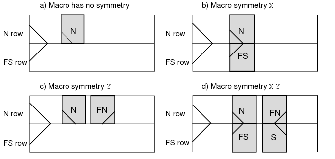
Example 1-27 Double-Height Cells
Double-height cells that are intended to align with flipped and abutted single-height rows should have SITE symmetry X Y and MACRO symmetry X Y. These symmetries allow all four cell orientations (N, FN, FS, and S) to fit inside the double-height row (see Figure 1-40 ). Usually, double-height rows are just N orientation rows that are abutted and aligned with a pair of single-height flipped and abutted rows.
Figure 1-40 Legal Placements for Single-Height Row Sites with Symmetry Y and Double-Height Row Sites with Symmetry X Y
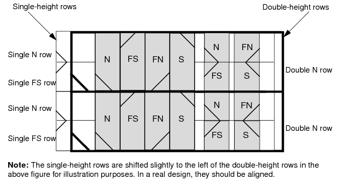
Example 1-28 Special Orientations
Some single-height cells have special orientation needs. For example, the design requires flipped and abutted rows, but only N and FS orientations are allowed because of the special layout of well taps on the right side of a group of cells that borrow from the left side of the next cell. That is, you cannot place an N and FN cell against each other in one row because only N cells are allowed in an N row. In this case, the SITE symmetry should not be defined, and the MACRO symmetry should be X. A MACRO symmetry of X Y can also be defined because the Y-flipped macros (FN and S orientations) do not match the N or FS rows. See Figure 1-41 for the different combinations when the SITE has no symmetry.
Figure 1-41 Legal Placements for Row Sites with No Symmetry
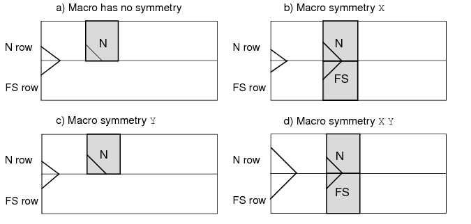
Example 1-29 Vertical Rows
Single-height sites are normally given symmetry X, and single-height cells are normally given symmetry X Y. Example d in Figure 1-42 shows the legal placement for a site with symmetry X, and the typical standard cell MACRO symmetry X Y.
Figure 1-42 Legal Placements for Vertical Row Sites With Symmetry X
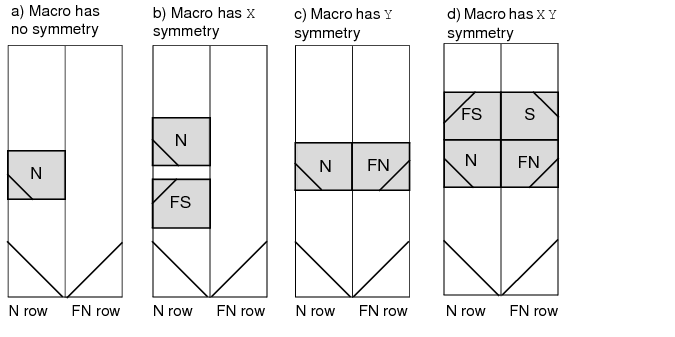
Used in the macro obstruction (OBS) and pin port (PIN) statements to define layer geometries in the design.
|
DESIGNRULEWIDTH value |
||
|
Specifies the effective design rule width. If specified, the obstruction or pin is treated as a shape of this width for all spacing checks. If you specify DESIGNRULEWIDTH, you cannot specify the SPACING argument. As a lot of spacing rules in advanced nodes no longer just rely on wire width, DESIGNRULEWIDTH is not allowed for 20nm and below nodes. |
||
|
Indicates that the obstruction shapes block signal routing, but do not block power or ground routing. This can be used to block signal routes that might cause noise, but allow connections to power and ground pins. |
||
|
Creates an array of the PATH, RECT, POLYGON, or VIA geometry, as specified by the given step pattern. ITERATE specifications simplify the definitions of cover macros. The syntax for stepPattern is defined as follows: DO numX BY numY STEP spaceX spaceY |
||
|
Specifies the spacing, in distance units, between the columns and rows of points. |
||
|
LAYER layerName |
Specifies the layer on which to place the geometry. Note: For macro obstructions, you can specify cut, implant, or overlap layers. |
|
|
MASK maskNum |
Specifies which mask from double- or triple-patterning to use for this shape. The maskNum variable must be a positive integer. Most applications only support values of 1, 2, or 3. Shapes without any defined mask have no mask set (they are considered uncolored). The uncolored PIN shapes can be assigned to an arbitrary mask as long as they do not have a spacing conflict with neighbor objects. The meaning of uncolored OBS shapes depends on the cell. For standard cell MACROs (with a SITE that is CLASS CORE), the uncolored OBS shapes are considered to be real metal shapes that can be assigned to any mask as long as no mask spacing conflicts occur. For other MACRO types, uncolored OBS shapes are assumed to be abstractions that may be any mask, so other shapes must be spaced far enough away to avoid a violation to any mask shape at that location. |
|
|
MASK viaMaskNum |
The viaMaskNum is a hex-encoded 3 digit value of the form: <topMaskNum><cutMaskNum><bottomMaskNum> For example, MASK 113 means the top metal and cut layer maskNum is 1, and the bottom metal layer maskNum is 3. A value of 0 means the shape on that layer has no mask assignment (is uncolored), so 013 means the top layer is uncolored. If either the first or second digit is missing, they are assumed to be 0, so 013 and 13 means the same thing. Most applications only support maskNum values of 0, 1, 2, or 3 for double or triple patterning. |
|
|
The topMaskNum and bottomMaskNum variables specify which mask the corresponding metal shape belongs to. The via-master metal mask values have no effect. For the cut-layer, the cutMaskNum defines the mask for the bottommost, and then the leftmost cut. For multi-cut vias, the via-instance cut masks are derived from the via-master cut mask values. The via-master must have a mask defined for all of the cut shapes and every via-master cut mask is "shifted" (1 to 2, 2 to 1 for two mask layers, and 1 to 2, 2 to 3, 3 to 1 for three mask layers) so the lower-left cut matches the cutMaskNum value. See Example 1-31 . Similarly, for the metal layer, the topMaskNum/bottomMaskNum would define the mask for the bottom-most, then leftmost metal shape. For multiple disjoint metal shapes, the via-instance metal masks are derived from the via-master metal mask values. The via-master must have a mask defined for all of the metal shapes, and every via-master metal mask is "shifted" (1->2, 2->1 for two mask layers, 1->2, 2->3, 3->1 for three mask layers) so the lower-left cut matches the topMaskNum/bottomMaskNum value. |
||
|
PATH pt |
Creates a path between the specified points, such as pt1 pt2 pt3. The path automatically extends the length by half of the current width on both endpoints to form a rectangle. (A previous WIDTH statement is required.) The line between each pair of points must be parallel to the x or y axis (45-degree angles are not allowed). You can also specify a path with a single coordinate, in which case a square whose side is equal to the current width is placed with its center at pt. |
|
|
POLYGON pt pt pt pt |
||
|
Specifies a sequence of at least three points to generate a polygon geometry. Every polygon edge must be parallel to the x or y axis, or at a 45-degree angle. Each POLYGON statement defines a polygon generated by connecting each successive point, and then by connecting the first and last points. |
||
|
RECT pt pt |
Specifies a rectangle, where the two points specified are opposite corners of the rectangle. There is no functional difference between a geometry specified using PATH and a geometry specified using RECT. |
|
|
SPACING minSpacing |
Specifies the minimum spacing allowed between this particular OBS and any other shape. While the syntax is shared for both OBS and PIN, it is only intended to be used with OBS shapes. The minSpacing value overrides all other normal LAYER-based spacing rules, including wide-wire spacing rules, end-of-line rules, parallel run-length rules, etc. An OBS with SPACING is not "seen" by any other DRC check, except the simple check for minSpacing to any other routing shape on the same layer. One common application is to put an OBS SPACING 0 shape on top of some PIN shapes to restrict the access of a router to other parts of the PIN without the OBS shape. This is sometimes needed for cells with large drive strengths to avoid electromigration problems by restricting the router to connect only to the middle of the output pin. The minSpacing value cannot be larger than the maximum spacing defined in the SPACING or SPACINGTABLE for that layer. Tools may change larger values to the maximum spacing value with a warning. |
|
|
VIA pt viaName |
||
|
WIDTH width |
Specifies the width that the PATH statements use. If you do not specify width, the default width for that layer is used. When you specify a width, that width remains in effect until the next WIDTH or LAYER statement. When another LAYER statement is given, the WIDTH is automatically reset to the default width for that layer. |
|
Example 1-30 Layer Geometries
The following example shows how to define a set of geometries, first by using ITERATE statements, then by using individual PATH, VIA and RECT statements.
The following two sets of statements are equivalent:
PATH ITERATE 532.0 534 1999.2 534
DO 1 BY 2 STEP 0 1446 ;
VIA ITERATE 470.4 475 VIABIGPOWER12
DO 2 BY 2 STEP 1590.4 1565 ;
RECT ITERATE 24.1 1.5 43.5 16.5
DO 2 BY 1 STEP 20.0 0 ;
PATH 532.0 534 1999.2 534 ;
PATH 532.0 1980 1999.2 1980 ;
VIA 470.4 475 VIABIGPOWER12 ;
VIA 2060.8 475 VIABIGPOWER12;
VIA 470.4 2040 VIABIGPOWER12;
VIA 2060.8 2040 VIABIGPOWER12;
RECT 24.1 1.5 43.5 16.5 ;
RECT 44.1 1.5 63.5 16.5 ;
Example 1-31 Layer Geometries - multi-mask patterns
The following example shows how to use multi-mask patterns:
LAYER M1 ;
RECT MASK 2 10 10 11 11 ;
LAYER M2 ;
RECT 10 10 11 11 ;
VIA 5 5 VIA1_1 ;
VIA MASK 031 15 15 VIA1_2 ;
|
|
M1 rect shape belongs to MASK 2 |
|
|
M2 rect shape has no mask set |
|
|
VIA1_1 via has no mask set (all the metal and cut shapes have no mask) |
|
|
VIA1_2 via will have: |
|
|

|
No mask set for the top metal shape (topMaskNum is 0 in the 031 value) |
|
|
|
MASK 1 for the bottom metal shape (botMaskNum is 1 in the 031 value) |
|
|
|
The bottommost, and then the leftmost cut of the via-instance is MASK 3. The mask for the other cuts of the via-instance are derived from the via-master by "shifting" the via-master cut masks to match. So if the via-master's bottomleft cut is MASK 1, then the via-master cuts on MASK 1 become MASK 3 for the via-instance, and similarly cuts on 2 to 1, and cuts on 3 to 2. See Figure 1-43. |
LAYER M1 ;
RECT MASK 2 10 10 11 11 ;
LAYER M2 ;
RECT 10 10 11 11 ;
VIA 5 5 VIA1_1 ;
VIA MASK 031 15 15 VIA1_2 ;
Figure 1-43 Via-master multi-mask patterns
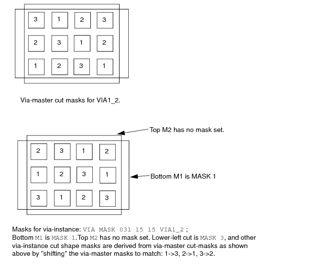
Defines a set of obstructions (also called blockages) on the macro. You specify obstruction geometries using the layer geometry syntax. See "Layer Geometries" for syntax information.
Normally, obstructions block routing, except for when a pin port overlaps an obstruction (a port geometry overrules an obstruction). For example, you can define a large rectangle for a metal1 obstruction and have metal1 port in the middle of the obstruction. The port can still be accessed by a via, if the via is entirely inside the port.
In Figure 1-44 , the router can only access the metal1 port from the right. If the metal2 obstruction did not exist, the router could connect to the port with a metal12 via, as long as the metal1 part of the via fit entirely inside the metal1 port.
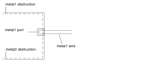
Routing can also connect to such a port on the same layer if the routing does not cross any obstruction by more than a distance of the total of minimum width plus minimum spacing before reaching the pin. This is because the port geometry is known to be "real," and any obstruction less than a distance of minimum width plus minimum spacing away from the port is not a real obstruction. If the pin is more than minimum width plus minimum spacing away from the obstruction edge, the router can only route to the pin from the layer above or below using a via (see Figure 1-45 ).
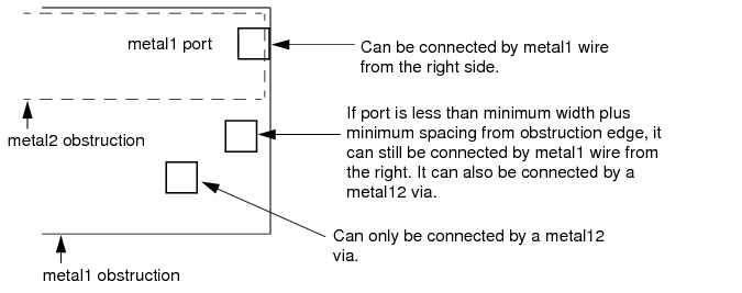
Significant routing time can be saved if obstructions are simplified. Especially in metal1, construct obstructions so that free tracks on the layer are accessible to the router. If most of the routing resource is obstructed, simplify the obstruction modeling by combining small obstructions into a single large obstruction. For example, use the bounding box of all metal1 objects in the cell, rather than many small obstructions, as the bounding box of the obstruction.
You must be sure to model via obstructions over the rest of the cell properly. A single, large cut12 obstruction over the rest of the cell can do this in some cases, as when metal1 resource exists within the cell outside the power buses.
Describe a rectilinear footprint by setting the SIZE of the macro as a whole to a rectangular bounding box, then defining obstructions within the bounding box on the overlap layer. The obstructions on the overlap layer indicate areas within the bounding box which no other macro should overlap. The obstructions should completely cover the rectilinear shape of the macro, but not the portion of the bounding box that might overlap with other macros during placement.
Note: Specify the overlaps for the macro using the OBS statement. To do this, specify a layer of type OVERLAP and then give the overlap geometries, as shown in Figure 1-46.
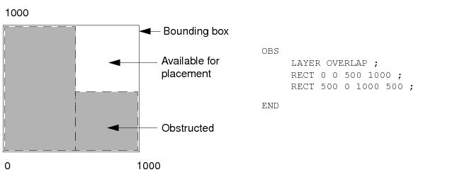
Defines pins for the macro. PIN statements must be included in the LEF specification for each macro. All pins, including VDD and VSS, must be specified. The first pin listed becomes the first pin in the database. List the pins in the following order:
ANTENNADIFFAREA value [LAYER layerName]
Specifies the diffusion (diode) area, in micron-squared units, to which the pin is connected on a layer. If you do not specify a layer name, the value applies to all layers. For more information on process antenna calculation, see Appendix C, "Calculating and Fixing Process Antenna Violations."
ANTENNAGATEAREA value [LAYER layerName]
Specifies the gate area, in micron-squared units, to which the pin is connected on a layer. If you do not specify a layer name, the value applies to all layers. For more information on process antenna calculation, see Appendix C, "Calculating and Fixing Process Antenna Violations."
ANTENNAMAXAREACAR value LAYER layerName
For hierarchical process antenna effect calculation, specifies the maximum cumulative area ratio value on the specified layerName, using the metal area at or below the current pin layer, excluding the pin area itself. This is used to calculate the actual cumulative antenna ratio on the pin layer, or the layer above it.
For more information on process antenna calculation, see Appendix C, "Calculating and Fixing Process Antenna Violations."
ANTENNAMAXCUTCAR value LAYER layerName
For hierarchical process antenna effect calculation, specifies the maximum cumulative antenna ratio value on the specified layerName, using the cut area at or below the current pin layer, excluding the pin area itself. This is used to calculate the actual cumulative antenna ratio for the cuts above the pin layer.
For more information on process antenna calculation, see Appendix C, "Calculating and Fixing Process Antenna Violations."
ANTENNAMAXSIDEAREACAR value LAYER layerName
For hierarchical process antenna effect calculation, specifies the maximum cumulative antenna ratio value on the specified layerName, using the metal side wall area at or below the current pin layer, excluding the pin area itself. This is used to calculate the actual cumulative antenna ratio on the pin layer or the layer above it.
For more information on process antenna calculation, see Appendix C, "Calculating and Fixing Process Antenna Violations."
ANTENNAMODEL {OXIDE1 | OXIDE2 | OXIDE3 | OXIDE4}
Specifies the oxide model for the pin. If you specify an ANTENNAMODEL statement, the value affects all ANTENNAGATEAREA and ANTENNA*CAR statements for the pin that follow it until you specify another ANTENNAMODEL statement. The ANTENNAMODEL statement does not affect ANTENNAPARTIAL*AREA and ANTENNADIFFAREA statements because they refer to the total metal, cut, or diffusion area connected to the pin, and do not vary with each oxide model.
Default: OXIDE1, for a new PIN statement
Because LEF is often used incrementally, if an ANTENNA statement occurs twice for the same oxide model, the last value specified is used.
For most standard cells, there is only one value for the ANTENNAPARTIAL*AREA and ANTENNADIFFAREA values per pin; however, for a block with six routing layers, it is possible to have six different ANTENNAPARTIAL*AREA values and six different ANTENNAPINDIFFAREA values per pin. It is also possible to have six different ANTENNAPINGATEAREA and ANTENNAPINMAX*CAR values for each oxide model on each pin.
Example 1-32 Pin Antenna Model
The following example describes oxide model information for pins IN1 and IN2.
PIN IN1
ANTENNADIFFAREA 1.0 ; #not affected by ANTENNAMODEL
...
ANTENNAMODELOXIDE OXIDE1 ; #OXIDE1 not required, but is good
#practice
ANTENNAGATEAREA 1.0 ; #OXIDE1 gate area
ANTENNAMAXAREACAR 50.0 LAYER m1 ; #metal1 CAR value
...
ANTENNAMODEL OXIDE2 ; #OXIDE2 starts here
ANTENNAGATEAREA 3.0 ; #OXIDE2 gate area
...
PIN IN2
ANTENNADIFFAREA 2.0 ; #not affected by ANTENNAMODEL
ANTENNAPARTIALMETALAREA 2.0 LAYER m1 ;
...
#no OXIDE1 specified for this pin
ANTENNAMODEL OXIDE2 ;
ANTENNAGATEAREA 1.0 ;
...
ANTENNAPARTIALCUTAREA value [LAYER layerName]
Specifies the partial cut area above the current pin layer and inside the macro cell on the layer. For a hierarchical design, only the cut layer above the I/O pin layer is needed for partial antenna ratio calculation. If you do not specify a layer name, the value applies to all layers.
For more information on process antenna calculation, see Appendix C, "Calculating and Fixing Process Antenna Violations."
ANTENNAPARTIALMETALAREA value [LAYER layerName]
Specifies the partial metal area connected directly to the I/O pin and the inside of the macro cell on the layer. For a hierarchical design, only the same metal layer as the I/O pin, or the layer above it, is needed for partial antenna ratio calculation. If you do not specify a layer name, the value applies to all layers.
For more information on process antenna calculation, see Appendix C, "Calculating and Fixing Process Antenna Violations."
Note: Metal area is calculated by adding the pin's geometric metal area and the ANTENNAPARTIALMETALAREA value.
ANTENNAPARTIALMETALSIDEAREA value [LAYER layerName]
Specifies the partial metal side wall area connected directly to the I/O pin and the inside of the macro cell on the layer. For a hierarchical design, only the same metal layer as the I/O pin or the layer above is needed for partial antenna ratio calculation. If you do not specify a layer name, the value applies to all layers.
For more information on process antenna calculation, see Appendix C, "Calculating and Fixing Process Antenna Violations."
DIRECTION {INPUT | OUTPUT [TRISTATE] | INOUT | FEEDTHRU}
Specifies the pin type. Most current tools do not usually use this keyword. Typically, pin directions are defined by timing library data, and not from LEF.
Default: INPUT
Value: Specify one of the following:
|
Pin that drives signals out of the cell. The optional TRISTATE argument indicates tristate output pins for ECL designs. |
||
|
Pin that can accept signals going either in or out of the cell. |
||
GROUNDSENSITIVITY groundPinName
Specifies that if this pin is connected to a tie-low connection (such as 1'b0 in Verilog), it should connect to the same net to which groundPinName is connected.
groundPinName must match a pin on this macro that has a USE GROUND attribute. The ground pin definition can follow later in this MACRO statement; it does not have to be defined before this pin definition. For an example, see Example 1-33.
Note: GROUNDSENSITIVITY is useful only when there is more than one ground pin in the macro. By default, if there is only one USE GROUND pin, then the tie-low connections are already implicitly defined (that is, tie-low connections are connected to the same net as the one ground pin).
MUSTJOIN pinName
Specifies the name of another pin in the cell that must be connected with the pin being defined. MUSTJOIN pins provide connectivity that must be made by the router. In the LEF file, each pin referred to must be defined before the referring pin. The remaining MUSTJOIN pins in the set do not need to be defined contiguously.
Note: MUSTJOIN pin names are never written to the DEF file; they are only used by routers to add extra connection points during routing.
|
MUSTJOIN pins have the following restrictions:
|
Schematic and nonschematic MUSTJOIN pins are handled in slightly different ways. For schematic MUSTJOIN pins, the pins are added to the pin set for the (unique) net associated with the ring for each component instance of the macro. The net is routed in the usual manner, and routing data for the MUSTJOIN pins are included in routing data for the net.
The mustjoin routing is not necessarily performed before the rest of the net. Timing relations should not be given for MUSTJOIN pins, and internal mustjoin routing is modeled as lumped capacitance at the schematic pin.
Nonschematic MUSTJOIN pin sets get routed in the usual manner. However, when the DEF file is outputted, routing data is reported in the NETS section of the file as follows:
MUSTJOIN compName pinName + regularWiring ;
Here, compName is the component and pinName is an arbitrary pin in the set. You can also use the preceding to input prewiring for the MUSTJOIN pin, using FIXED or COVER.
NETEXPR "netExprPropName defaultNetName"
Specifies a net expression property name (such as power1 or power2) and a default net name. If netExprPropName matches a net expression property in the netlist (such as in Verilog, VHDL, or OpenAccess), then the property is evaluated, and the software identifies a net to which to connect this pin. If this property does not exist, defaultNetName is used for the net name.
netExprPropName must be a simple identifier in order to be compatible with other languages, such as Verilog and CDL. Therefore, it can only contain alphanumeric characters, and the first character cannot be a number. For example, power2 is a legal name, but 2power is not. You cannot use characters such as $ and !. The defaultName can be any legal DEF net name.
Example 1-33 Net Expression and Supply Sensitivity
The following statement defines sensitivity and net expression values for four pins on the macro myMac:
...
PIN in1
...
SUPPLYSENSITIVITY vddpin1 ; #If in1 is 1'b1, use net connected to vddpin1.
#Note that no GROUNDSENSITIVITY is needed
#because only one ground pin exists.
#Therefore, 1'b0 implicitly means net from
#pin gndpin.
...
END in1
PIN vddpin1
...
NETEXPR "power1 VDD1" ; #If power1 net expression is defined in the
#netlist, use it to find the net connection. If
#not, use net VDD1.
...
END vddpin1
PIN vddpin2
...
NETEXPR "power2 VDD2" ; #If power2 net expression is defined in the
#netlist, use it to find the net connection.If
#not, use net VDD2.
...
END vddpin2
PIN gndpin
...
NETEXPR "gnd1 GND" ; #If gnd1 net expression is defined in the
#netlist, use it to find the net connection. If
#not, use net GND.
...
END gndpin
...
PIN pinName
Specifies the name for the library pin.
Starts a pin port statement that defines a collection of geometries that are electrically equivalent points (strongly connected). A pin can have multiple ports. Each PORT of the same PIN is considered weakly connected to the other PORTs, and should already be connected inside the MACRO (often through a resistive path).
Strongly connected shapes (that is, multiple shapes of one PORT) indicate that a signal router is allowed to connect to one shape of the PORT, and continue routing from another shape of the same PORT.
Weakly connected shapes (that is, separate PORTs of the same PIN) are assumed to be connected through resistive paths inside the MACRO that should not be used by routers. The signal router should connect to one or the other PORT, but not both.
Power routers should connect to every PORT statement, if there is more than one for a given PIN. For example, if a block has several PORTs on the boundary for the VSS PIN, each PORT should be connected by the power router.
The syntax for describing pin port statements is defined as follows:
{PORT
[CLASS {NONE | CORE | BUMP} ;]
{layerGeometries} ...
END} ...
|
Specifies the port type. A port can be one of the following: BUMP--Specifies the port is a bump connection point. A bump port should only be connected by routing to a bump (normally a MACRO CLASS COVER BUMP cell). CORE--Specifies the port is a core ring connection point. A core port is used only on power and ground I/O drivers used around the periphery. The core port indicates which power or ground port to connect to a core ring for the chip (inside the I/O pads). NONE--Specifies the port is a default port that is connected by normal "default" routing. NONE is the default value if no PORT CLASS statement is specified. |
||
|
Defines port geometries for the pin. You specify port geometries using layer geometries syntax. See "Layer Geometries" for syntax information. |
||
PROPERTY propName propVal
Specifies a numerical or string value for a pin property defined in the PROPERTYDEFINITIONS statement. The propName you specify must match the propName listed in the PROPERTYDEFINITIONS statement.
You can create a via in pin only rule by using the following property definition:
Specifies that vias must be dropped inside the original pin shapes to connect to the pin, and planar connection to the pin is not allowed. In some advanced nodes, the pin shapes can be extended for metal alignment purpose. However, via insertion is not allowed in that extended portion.
Specifies a pin with special connection requirements because of its shape.
Value: Specify one of the following:
|
Pin with an irregular shape with a jog or neck within the cell. |
||
|
Figure 1-47 shows an example of an abutment and a feedthrough pin. Note: When you define feedthrough and abutment pins for use with power routing, you must do the following: |
||
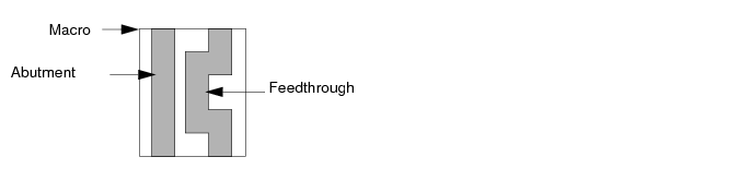
SUPPLYSENSITIVITY powerPinName
Specifies that if this pin is connected to a tie-high connection (such as 1'b1 in Verilog), it should connect to the same net to which powerPinName is connected.
powerPinName must match a pin on this macro that has a USE POWER attribute. The power pin definition can follow later in this MACRO statement; it does not have to be defined before this pin definition. For an example, see Example 1-33.
Note: SUPPLYSENSITIVITY is useful only when there is more than one power pin in the macro. By default, if there is only one USE POWER pin, then the tie-high connections are already implicitly defined (that is, tie-high connections are connected to the same net as the one power pin).
TAPERRULE ruleName
Specifies the nondefault rule to use when tapering wires to the pin.
USE {ANALOG | CLOCK | GROUND | POWER | SIGNAL}
Specifies how the pin is used. Pin use is required for timing analysis.
Default: SIGNAL
Value: Specify one of the following:
|
Pin is used for connectivity to the chip-level ground distribution network. |
||
|
Pin is used for connectivity to the chip-level power distribution network. |
||
Specifies the value for the manufacturing grid, in microns. value must be a positive number.
Type: Float
Specifies the maximum number of single-cut stacked vias that are allowed on top of each other (that is, in one continuous stack). A via is considered to be in a stack with another via if the cut of the first via overlaps any part of the cut of the second via. A double-cut or larger via interrupts the stack. For example, a via stack consisting of single via12, single via23, double-cut via34, and single via45 has a single-cut stack of height 2 for via12 and via23, and a single-cut stack of height 1 for via45 because the full stack is broken up by double-cut via34.
The MAXVIASTACK statement should follow the LAYER statements in the LEF file; however, it is not attached to any particular layer. You can specify only one MAXVIASTACK statement in a LEF file.
RANGE bottomLayer topLayer
Specifies a range of layers for which the maximum stacked via rule applies. If you do not specify a range, the value applies for all layers.
Specifies the maximum allowed number of single-cut stacked vias.
Type: Integer
Example 1-34 Maximum Via Stack Statement
The following MAXVIASTACK statement specifies that only four stacked vias are allowed on top of each other. This rule applies to all layers.
...
If you specify the following statement instead, the stacked via limit applies only to layers metal1 through metal7.
Note: Use the VIA statement to define vias for nondefault wiring.
DIAGWIDTH diagWidth
Specifies the diagonal width for layerName, when 45-degree routing is used.
Default: The minimum width value (WIDTH minWidth)
Type: Float, specified in microns
Specifies that any spacing values that exceed the LEF LAYER spacing requirements are "hard" rules instead of "soft" rules. By default, routers treat extra spacing requirements as soft rules that are high cost to violate, but not real spacing violations. However, in certain situations, the extra spacing should be treated as a hard, or real, spacing violation, such as when the route will be modified with a post-process that replaces some of the extra space with metal.
LAYER layerName ... END layerName
Specifies the layer for the various width and spacing values. This layer must be a routing layer. Every routing layer must have a WIDTH keyword and value specified. All other keywords are optional.
MINCUTS cutLayerName numCuts
Specifies the minimum number of cuts allowed for any via using the specified cut layer. Routers should only use vias (generated or predefined fixed vias) that have at least numCuts cuts in the via.
Type: (numCuts) Positive integer
NONDEFAULTRULE ruleName
Specifies a name for the new routing rule. The name DEFAULT is reserved for the default routing rule used by most nets. The default routing rule is constructed automatically from the LEF LAYER statement WIDTH, DIAGWIDTH, SPACING, and WIREEXTENSION values, from the LEF VIA statement (any vias with the DEFAULT keyword), and from the LEF VIARULE statement (any via rules with the DEFAULT keyword). If you specify DEFAULT for ruleName, the automatic creation is overridden, and the default routing rule is defined directly from this rule definition.
PROPERTY propName propValue
Specifies a numerical or string value for a nondefault rule property defined in the PROPERTYDEFINITIONS statement. The propName you specify must match the propName listed in the PROPERTYDEFINITIONS statement.
SPACING minSpacing
Specifies the recommended minimum spacing for layerName of routes using this NONDEFAULTRULE to other geometries. If the spacing is given, it must be at least as large as the foundry minimum spacing rules defined in the LAYER definitions. Routers should attempt to meet this recommended spacing rule; however, the spacing rule can be relaxed to the foundry spacing rules along some parts of the wire if the routing is very congested, or if it is difficult to reach a pin.
Adding extra space to a nondefault rule allows a designer to reduce cross-coupling capacitance and noise, but a clean route with no actual foundry spacing violations will still be allowed, unless the HARDSPACING statement is specified.
Type: Float, specified in microns
USEVIA viaName
Specifies a previously defined via from the LEF VIA statement, or a previously defined NONDEFAULTRULE via to use with this routing rule.
USEVIARULE viaRuleName
Specifies a previously defined VIARULE GENERATE rule to use with this routing rule. You cannot specify a rule from a VIARULE without a GENERATE keyword.
VIA viaStatement
Defines a new via. You define nondefault vias using the same syntax as default vias. For syntax information, see "Via". All vias, default and nondefault, must have unique via names. If you define more than one via for a rule, the router chooses which via to use.
Note: Defining a new via is no longer recommended, and is likely to become obsolete. Instead, vias should be predefined in a LEF VIA statement, then added to the nondefault rule using the USEVIA keyword.
WIDTH width
Specifies the required minimum width for layerName.
Type: Float, specified in microns
WIREEXTENSION value
Specifies the distance by which wires are extended at vias. Enter 0 (zero) to specify no extension. Values other than 0 must be greater than or equal to half of the routing width for the layer, as defined in the nondefault rule.
Default: Wires are extended half of the routing width
Type: Float, specified in microns
Note: The WIREEXTENSION statement only extends wires and not vias. For 65nm and below, WIREEXTENSION is no longer recommended because it may generate some advance rule violations if wires and vias have different widths. See Illustration of WIREEXTENSION.
Example 1-35 Nondefault Rule Statement
Assume two default via rules were defined:
VIARULE via12rule GENERATE DEFAULT
LAYER metal1 ;
...
VIARULE via23rule GENERATE DEFAULT
LAYER metal2 ;
...
|
|
Assuming the minimum width is 1.0 μm, the following nondefault rule creates a 1.5x minimum width wire using default spacing: |
LAYER metal1
WIDTH 1.5 ; #metal1 has a 1.5 um width
END metal1
LAYER metal2
WIDTH 1.5 ;
END metal2
LAYER metal3
WIDTH 1.5 ;
END metal3
Note: If there were no default via rules, then a VIA, USEVIA, or USEVIARULE keyword would be required. Because there are none defined, the default via rules are implicitly inherited for this nondefault rule; therefore, via12rule and via23rule would be used for this routing rule.
LAYER metal1
WIDTH 3.0 ; #metal1 has 3.0 um width
END metal1
LAYER metal2
WIDTH 3.0 ;
END metal2
LAYER metal3
WIDTH 3.0 ;
END metal3
#viarule12 and viarule23 are used implicitly
MINCUTS cut12 2 ; #at least two-cut vias are required for cut12
MINCUTS cut23 2 ;
HARDSPACING ; #do not let any other signal close to this one
LAYER metal1
WIDTH 1.5 ; #metal1 has 1.5 um width
SPACING 3.0 ; #extra spacing of 3.0 um
END metal1
LAYER metal2
WIDTH 1.5
SPACING 3.0
END metal2
LAYER metal3
WIDTH 1.5
SPACING 3.0
END metal3
#Use predefined "analog vias"
#The DEFAULT VIARULES will not be inherited.
USEVIA via12_fixed_analog_via ;
USEVIA via_23_fixed_analog_via ;
Lists all properties used in the LEF file. You must define properties in the PROPERTYDEFINITIONS statement before you can refer to them in other sections of the LEF file.
Specifies the object type being defined. You can define properties for the following object types:
Specifies a unique property name for the object type.
Specifies the property type for the object type. You can specify one of the following property types:
RANGE min max
Limits real number and integer property values to a specified range. That is, the value must be greater than or equal to min and less than or equal to max.
value | "stringValue"
Assigns a numeric value or a name to a LIBRARY object type.
Note: Assign values to other properties in the section of the LEF file that describes the object to which the property applies.
Example 1-36 Property Definitions Statement
The following example shows library, via, and macro property definitions.
LIBRARY versionNum INTEGER 12;
LIBRARY title STRING "Cadence96";
VIA count INTEGER RANGE 1 100;
MACRO weight REAL RANGE 1.0 100.0;
MACRO type STRING;
Defines a placement site in the design. A placement site gives the placement grid for a family of macros, such as I/O, core, block, analog, digital, short, tall, and so forth. SITE definitions can be used in DEF ROW statements.
|
Specifies whether the site is an I/O pad site or a core site. |
||
|
ROWPATTERN {previousSiteName siteOrient} |
||
|
Specifies a set of previously defined sites and their orientations that together form siteName. |
||
|
Specifies the name of a previously defined site. The height of each previously defined site must be the same as the height specified for siteName, and the sum of the widths of the previously defined sites must equal the width specified for siteName. |
||
|
Specifies the orientation for the previously defined site. This value must be one of N, S, E, W, FN, FS, FE, and FW. For more information on orientations, see "Specifying Orientation" in the DEF COMPONENT section. |
||
Example 1-37 Site Row Pattern Statement
The following example defines three sites: Fsite; Lsite; and mySite, which consists of a pattern of Fsite and Lsite sites:
CLASS CORE ;
SIZE 4.0 BY 7.0 ; #4.0 um width, 7.0 um height
CLASS CORE ;
SIZE 6.0 BY 7.0 ; #6.0 um width, 7.0 um height
ROWPATTERN Fsite N Lsite N Lsite FS ; #Pattern of F + L + flipped L
SIZE 16.0 BY 7.0 ; #Width = width(F + L + L)
Figure 1-48 illustrates some DEF rows made up of mySite sites.
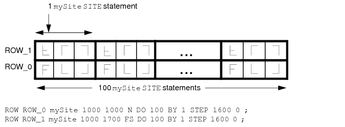
|
SITE siteName |
||
|
SIZE width BY height |
||
|
Specifies the dimensions of the site in normal (or north) orientation, in microns. |
||
|
Indicates which site orientations are equivalent. The sites in a given row all have the same orientation as the row. Generally, site symmetry should be used to control the flipping allowed inside the rows. For more information on defining symmetry, see "Defining Symmetry". |
||
|
X Y |
||
|
Site is symmetric when rotated 90 degrees. Typically, this value is not used. |
||
|
Note: Typically, a site for single-height standard cells uses symmetry Y, and a site for double-height standard cells uses symmetry X Y. |
||
Defines the units of measure in LEF. The values tell you how to interpret the numbers found in the LEF file. Units are fixed with a convertFactor for all unit types, except database units and capacitance. For more information, see "Convert Factors". Currently, other values for convertFactor appearing in the UNITS statement are ignored.
The UNITS statement is optional and, when used, must precede the LAYER statements.
|
CAPACITANCE PICOFARADS convertFactor |
||
|
CURRENT MILLIAMPS convertFactor |
||
|
DATABASE MICRONS LEFconvertFactor |
||
|
Interprets one LEF distance unit as multiplied when converted into database units. If you omit the DATABASE MICRONS statement, a default value of 100 is recorded as the LEFconvertFactor in the database. In this case, one micron would equal 100 database units. |
||
|
FREQUENCY MEGAHERTZ convertFactor |
||
|
POWER MILLIWATTS convertFactor |
||
|
RESISTANCE OHMS convertFactor |
||
|
TIME NANOSECONDS convertFactor |
||
|
VOLTAGE VOLTS convertFactor |
||
LEF supports values of 100, 200, 400, 800, 1000, 2000, 4000, 8000, 10,000, and 20,000 for LEFconvertFactor. The following table illustrates the conversion of LEF distance units into database units.
Defines how minimum spacing is calculated for obstruction (blockage) geometries.
|
Specifies how to calculate minimum spacing for obstruction geometries (MACRO OBS shapes). |
||
|
Spacing is computed to MACRO OBS shapes as if they were actual routing shapes. A wide OBS shape would use wide wire spacing rules, and a thin OBS shapes would use thin wire spacing rules. |
||
|
Spacing is computed as if the MACRO OBS shapes were min-width wires. Some LEF models abstract many min-width wires as a single large OBS shape; therefore using wide wire spacing would be too conservative. |
||
|
Note: OFF is the recommended value to specify because it is a better abstract model for the various wide wire spacing rules that are more common at process nodes of 130nm and smaller. Certain older style LEF abstracts use ON, but it can have unexpected side effects (such as hidden DRC errors) if the abstracts are not created very carefully. You cannot mix both types of LEF abstracts at the same time. |
||
Specifies which version of the LEF syntax is being used. number is a string of the form major.minor[.subMinor], such as 5.8.
Note: Many applications default to the latest version of LEF/DEF supported by the application (which depends on how old the application is). The latest version as described by this document is 5.8. However, a default value of 5.8 is not formally part of the language definition; therefore, you cannot be sure that all applications use this default value. Also, because the default value varies with the latest version, you should not depend on this.
A fixed via is defined using rectangles or polygons, and does not use a VIARULE. The fixed via name must mean the same via in all associated LEF and DEF files.
A generated via is defined using VIARULE parameters to indicate that it was derived from a VIARULE GENERATE statement. For a generated via, the via name is only used locally inside this LEF file. The geometry and parameters are maintained, but the name can be freely changed by applications that use this via when writing out LEF and DEF files. For example, large blocks that include generated vias as part of the LEF MACRO PIN statement can define generated vias inside the same LEF file without concern about via name collisions in other LEF files.
Note: Use the VIARULE GENERATE statement to define special wiring.
CUTSIZE xSize ySize
Specifies the required width (xSize) and height (ySize) of the cut layer rectangles.
Type: Float, specified in microns
CUTSPACING xCutSpacing yCutSpacing
Specifies the required x and y spacing between cuts. The spacing is measured from one cut edge to the next cut edge.
Type: Float, specified in microns
Identifies the via as the default via between the defined layers. Default vias are used for default routing by the signal routers.
If you define more than one default via for a layer pair, the router chooses which via to use. You must define default vias between metal1 and masterslice layers if there are pins on the masterslice layers.
All vias consist of shapes on three layers: a cut layer and two routing (or masterslice) layers that connect through that cut layer. There should be at least one RECT or POLYGON on each of the three layers.
ENCLOSURE xBotEnc yBotEnc xTopEnc yTopEnc
Specifies the required x and y enclosure values for the bottom and top metal layers. The enclosure measures the distance from the cut array edge to the metal edge that encloses the cut array.
Type: Float, specified in microns
Note: It is legal to specify a negative number, as long as the resulting metal size is positive.
LAYER layerName
Specifies the layer on which to create the rectangles that make up the via. All vias consist of shapes on three layers: a cut layer and two routing (or masterslice) layers that connect through that cut layer. There should be at least one RECT or POLYGON on each of the three layers.
LAYERS botMetalLayer cutLayer topMetalLayer
Specifies the required names of the bottom routing (or masterslice) layer, cut layer, and top routing (or masterslice) layer. These layer names must be previously defined in layer definitions, and must match the layer names defined in the specified LEF viaRuleName.
MASK maskNum
Specifies which mask for double- or triple-patterning lithography is to be applied to the shapes defined in RECT or POLYGON of the via master. The maskNum variable must be a positive integer. Most applications only support values of 1, 2, or 3. For a fixed via made up of RECT or POLYGON statements, the cut-shapes should either be all colored or not colored at all. It is an error to have partially colored cuts for one via. Uncolored cut shapes should be automatically colored if the layer is a multi-mask layer.
The metal shapes with a shape per layer of the via-master do not need colors because the via instance has the mask color, but some readers will color them as mask 1 for internal consistency (see Figure 1-54 ). So a writer may write out MASK 1 for the metal shapes even if they are read in with no MASK value.
OFFSET xBotOffset yBotOffset xTopOffset yTopOffset
Specifies the x and y offset for the bottom and top metal layers. By default, the 0,0 origin of the via is the center of the cut array, and the enclosing metal rectangles. These values allow each metal layer to be offset independently. After the non-shifted via is computed, the metal layer rectangles are offset by adding the appropriate values--the x/y BotOffset values to the metal layer below the cut layer, and the x/ y TopOffset values to the metal layer above the cut layer. These offsets are in addition to any offset caused by the ORIGIN values.
Default: 0, for all values
Type: Float, specified in microns
ORIGIN xOffset yOffset
Specifies the x and y offset for all of the via shapes. By default, the 0,0 origin of the via is the center of the cut array, and the enclosing metal rectangles. After the non-shifted via is computed, all cut and metal rectangles are offset by adding these values.
Default: 0, for both values
Type: Float, specified in microns
PATTERN cutPattern
Specifies the cut pattern encoded as an ASCII string. This parameter is only required when some of the cuts are missing from the array of cuts, and defaults to "all cuts are present," if not specified.
For information on and examples of via cut patterns, see Creating Via Cut Patterns.
The cutPattern syntax uses "_" as a separator, and is defined as follows:
numRows_rowDefinition
[_numRows_rowDefinition] ...
The rowDefinition syntax is defined as follows:
{[RrepeatNumber]hexDigitCutPattern} ...
|
Specifies a single hexadecimal digit that encodes a 4-bit binary value, in which 1 indicates a cut is present, and 0 indicates a cut is not present. |
||
|
Specifies a single hexadecimal digit that indicates how many times to repeat hexDigitCutPattern. |
||
For parameterized vias (with + VIARULE ...), the cutPattern has an optional suffix added to allow three types of mask color patterns. The default mask color pattern (no suffix) is a checker-board defined as an alternating pattern starting with MASK 1 at the bottom left. Then the mask cycles left-to-right, and from bottom-to-top, as shown in Figure 1-52.The other two patterns supported are alternating rows, and alternating columns, see Figure 1-53.
The optional suffixes are:
<cut_pattern>_MR alternating rows
<cut_pattern>_MC alternating columns
POLYGON pt pt pt
Specifies a sequence of at least three points to generate a polygon geometry. The polygon edges must be parallel to the x axis, to the y axis, or at a 45-degree angle. Each POLYGON keyword defines a polygon generated by connecting each successive point, and then connecting the first and last points. The pt syntax corresponds to an x y coordinate pair, such as -0.2 1.0.
Type: Float, specified in microns
Example 1-38 Via Rules
The following via rule describes a non-shifted via (that is, a via with no OFFSET or ORIGIN parameters). There are two rows and three columns of via cuts. Figure 1-49 illustrates this via rule.
VIA myVia
VIARULE myViaRule ;
CUTSIZE 20 20 ; #xCutSize yCutSize
LAYERS metal1 cut12 metal2 ;
CUTSPACING 30 30 ; #xCutSpacing yCutSpacing
ENCLOSURE 20 50 50 20 ; #xBotEnc yBotEnc xTopEnc yTopEnc
ROWCOL 2 3 ;
END myVia
Figure 1-49 Via Rule
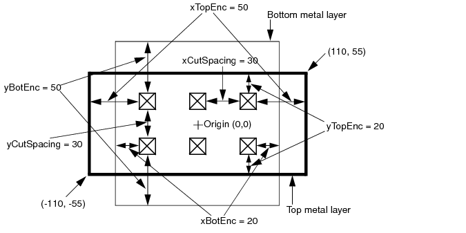
The same via rule with the following ORIGIN parameter shifts all of the metal and cut rectangles by 10 in the x direction, and by -10 in the y direction (see Figure 1-50 ):
ORIGIN 10 -10 ;
Figure 1-50 Via Rule With Origin
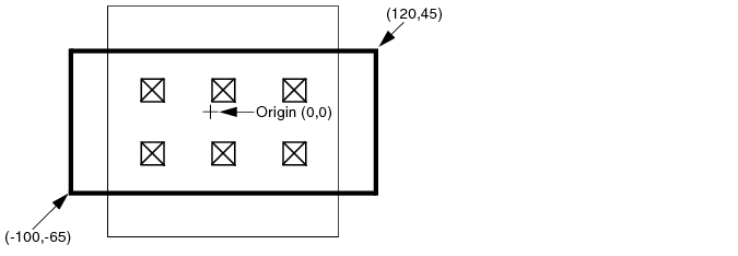
If the same via rule contains the following ORIGIN and OFFSET parameters, all of the rectangles shift by 10, -10. In addition, the top layer metal rectangle shifts by 20, -20, which means that the top metal shifts by a total of 30, -30.
ORIGIN 10 -10 ;
OFFSET 0 0 20 -20 ;
Figure 1-51 Via Rule With Origin and Offset
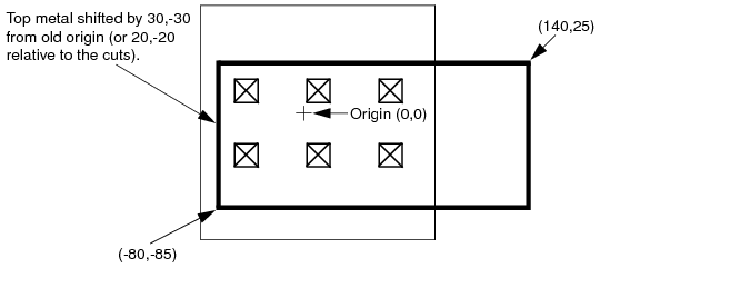
Example 1-39 Via Polygon
The following via definition creates a polygon geometry used by X-routing applications:
LAYER metal2 ;
POLYGON -2.1 -1.0 -0.2 1.0 2.1 1.0 0.2 -1.0 ;
LAYER cut23 ;
RECT -0.4 -0.4 0.4 0.4 ;
LAYER metal3 ;
POLYGON -0.2 -1.0 -2.1 1.0 0.2 1.0 2.1 -1.0 ;
|
PROPERTY propName propVal |
|
|
Specifies a numerical or string value for a via property defined in the PROPERTYDEFINITIONS statement. The propName you specify must match the propName listed in the PROPERTYDEFINITIONS statement. |
|
|
RECT pt pt |
Specify the corners of a rectangular shape in the via. The pt syntax corresponds to an x y coordinate pair, such as -0.4 -4.0. For vias used only in macros or pins, reference locations and rectangle coordinates must be consistent. |
|
RESISTANCE resistValue |
|
|
Specifies the lumped resistance for the via. This is not a resistance per via-cut value; it is the total resistance of the via. By default, via resistance is computed from the via LAYER RESISTANCE value; however, you can override that value with this value. resistValue is ignored if a via rule is specified, because only the VIARULE definition or a cut layer RESISTANCE value gives the resistance for generated vias. Note: A RESISTANCE value attached to an individual via is no longer recommended. |
|
|
ROWCOL numCutRows numCutCols |
|
|
Specifies the number of cut rows and columns that make up the via array. |
|
|
VIARULE viaRulename |
|
|
Specifies the name of the LEF VIARULE that produced this via. This indicates that the via is the result of automatic via generation, and that the via name is only used locally inside this LEF file. The geometry and parameters are maintained, but the name can be freely changed by applications that use this via when writing out LEF and DEF files. viaRuleName must be specified before you define any of the other parameters, and must refer to a previously defined VIARULE GENERATE rule name. It cannot refer to a VIARULE without a GENERATE keyword. Specifying the reserved via rule name of DEFAULT indicates that the via should use a previously defined VIARULE GENERATE rule with the DEFAULT keyword that exists for this routing-cut-routing (or masterslice-cut-masterslice) layer combination. This makes it possible for an IP block user to use existing via rules from the normal LEF technology section instead of requiring it to locally create its own via rules for just one LEF file. |
|
Example 1-40 Generated Via Rule
The following via definition defines a generated via that is used only in this LEF file.
VIARULE DEFAULT ; #Use existing VIARULE GENERATE rule with
#the DEFAULT keyword
CUTSIZE 0.1 0.1 ; #Cut is 0.1 x 0.1 um
LAYERS metal1 via12 metal2 ; #Bottom metal, cut, and top metal layers
CUTSPACING 0.1 0.1 ; #Space between cut edges is 0.1 um
ENCLOSURE 0.05 0.01 0.01 0.05 ; #metal1 enclosure is 0.05 in x, 0.01 in y
#metal2 enclosure is 0.01 in x, 0.05 in y
ROWCOL 1 2 ; #1 row, 2 columns = 2 cuts
Example 1-41 Parameterized via cut-mask pattern
The following example shows a VIARULE parameterized via:
VIA myParamVia1
VIARULE myGenVia1 CUTSIZE 0.4 0.4
LAYERS M1 VIA1 M2 CUTSPACING 0.4 0.4
ENCLOSURE 0.4 0 0 0.4 ROWCOL 3 4 #3 rows, 4 columns
PATTERN 2_F_1_D; #1 cut in top row is missing
Example of a parameterized via checker-board cut-mask pattern for a 3-mask layer with 2 missing cuts. For parameterized vias (with VIARULE ...), the mask of the cuts are pre-defined as an alternating pattern starting with MASK 1 at the bottom left. The mask cycles from left-to-right and bottom-to-top are shown.
Figure 1-52 Parameterized via cut-mask pattern using PATTERN
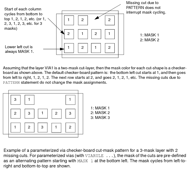
Figure 1-53 Parameterized via cut-mask pattern using Suffixes
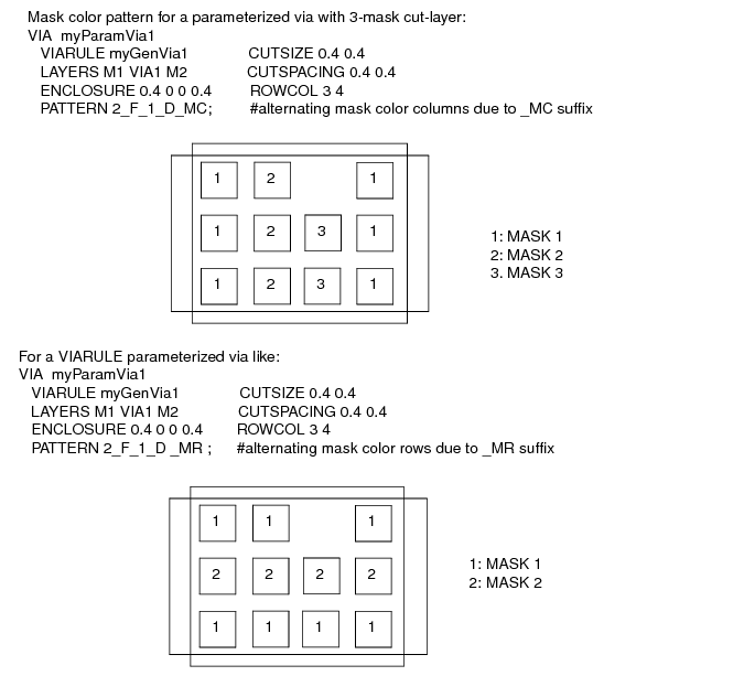
Example 1-42 Fixed-via with pre-colored cut shapes
The following example shows a fixed-via with pre-colored cut shapes:
VIA myVia1
LAYER m1 ;
RECT -0.4 -0.2 1.2 0.2 ; #no mask, some readers will set to mask 1
LAYER via1 ;
RECT MASK 1 -0.2 -0.2 0.2 0.2 ; #first cut on mask 1
RECT MASK 2 0.6 -0.2 1.0 0.2 ; #second cut on mask 2
LAYER m2 ;
RECT -0.2 -0.4 1.0 0.4 ; #no mask, some readers will set to mask 1
END myVia1
For a fixed via made up of RECT or POLYGON statements, the cut shapes must all be colored or not colored at all. If the cuts are not colored, they will be automatically colored in a checkerboard pattern as described above for parameterized vias. Each via-cut with the same lower-left Y value is considered one row, and each via in one row is a new column. For common "array" style vias with no missing cuts, this coloring is a good one. For vias that do not have a row and column structure, or are missing cuts this coloring may not be good (see Figure 1-54 ). If the metal layers having only one shape per layer are not colored, some applications will color them to MASK 1 for internal consistency, even though the via-master metal shape colors are not really used by LEF/DEF via instances. For multiple disjoint metal shapes, it is highly recommended to provide proper color.
Figure 1-54 Fixed-via with pre-colored cut shapes
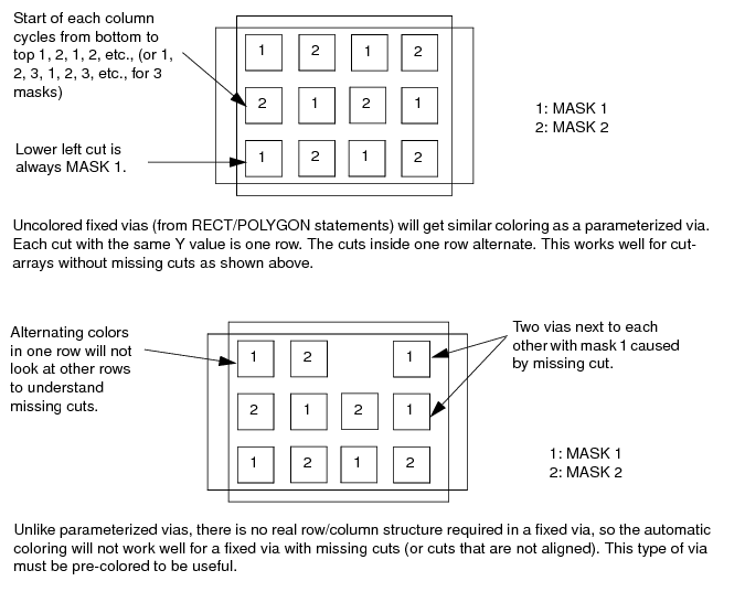
See the MACRO Layer Geometries statement to see how a via-instance uses these via-master mask values.
Defines which vias to use at the intersection of special wires of the same net.
Note: You should only use VIARULE GENERATE statements to create a via for the intersection of two special wires. In earlier versions of LEF, VIARULE GENERATE was not complete enough to cover all situations. In those cases, a fixed VIARULE (without a GENERATE keyword) was sometimes used. This is no longer required.
|
Specifies the wire direction. If you specify a WIDTH range, the rule applies to wires of the specified DIRECTION that fall within the range. Otherwise, the rule applies to all wires of the specified DIRECTION on the layer. |
|
|
LAYER layerName |
|
|
Specifies the routing or masterslice layers for the top or bottom of the via. |
|
|
PROPERTY propName propVal |
|
|
Specifies a numerical or string value for a via rules property defined in the PROPERTYDEFINITIONS statement. The propName you specify must match the propName listed in the PROPERTYDEFINITIONS statement. |
|
|
VIA viaName |
Specifies a previously defined via to test for the current via rule. The first via in the list that can be placed at the location without design rule violations is selected. The vias must all have exactly three layers in them. The three layers must include the same routing or masterslice layers as listed in the LAYER statements of the VIARULE, and a cut layer that is between the two routing or masterslice layers. |
|
VIARULE viaRuleName |
|
|
WIDTH minWidth TO maxWidth |
|
|
Specifies a wire width range. If the widths of two intersecting special wires fall within the wire width range, the VIARULE is used. To fall within the range, the widths must be greater than or equal to minWidth and less than or equal to maxWidth. Note: WIDTH is defined by wire direction, not by layer. If you specify a WIDTH range, the rule applies to wires of the specified DIRECTION that fall within the range. |
|
Example 1-43 Via Rule Statement
In the following example, whenever a metal1 wire with a width between 0.5 and 1.0 intersects a metal2 wire with a width between 1.0 and 2.0, the via generation code attempts to put a via12_1 at the intersection first. If the via12_1 causes a DRC violation, a via12_2 is then tried. If both fail, the default behavior from a VIARULE GENERATE statement for metal1 and metal2 is used.
LAYER metal1 ;
DIRECTION HORIZONTAL ;
WIDTH 0.5 TO 1.0 ;
LAYER metal2 ;
DIRECTION VERTICAL ;
WIDTH 1.0 TO 2.0 ;
VIA via12_1 ;
VIA via12_2 ;
Defines formulas for generating via arrays. You can use the VIARULE GENERATE statement to cover special wiring that is not explicitly defined in the VIARULE statement.
Note: Any vias created automatically from a VIARULE GENERATE rule that appear in the DEF NETS or SPECIALNETS sections must also appear in the DEF VIA section.
|
Specifies that the via rule can be used to generate vias for the default routing rule. There can only be one VIARULE GENERATE DEFAULT for a given routing-cut-routing (or masterslice-cut-masterslice) layer combination. |
||
Example 1-44 Via Rule Generate Default
VIARULE via12 GENERATE DEFAULT
LAYER m1 ;
ENCLOSURE 0.03 0.01 ; #2 sides need >= 0.03, 2 other sides need >= 0.01
LAYER m2 ;
ENCLOSURE 0.05 0.01 ; #2 sides need >= 0.05, 2 other sides need >= 0.01
LAYER cut12 ;
RECT -0.1 -0.1 0.1 0.1 ; # cut is .20 by .20
SPACING 0.40 BY 0.40 ; #center-to-center spacing
RESISTANCE 20 ; #ohms per cut
|
ENCLOSURE overhang1 overhang2 |
||
|
Specifies that the via must be covered by metal on two opposite sides by at least overhang1, and on the other two sides by at least overhang2 (see Figure 1-55 ). The via generation code then chooses the direction of overhang that best maximizes the number of cuts that can fit in the via. Note: If there are also ENCLOSURE rules for the cut layer that apply to a given via, the via generation code will choose the ENCLOSURE rule with values that match the ENCLOSURE in VIARULE GENERATE. If there is no such match, the via generation code will ignore the ENCLOSURE in VIARULE GENERATE and choose which ENCLOSURE rule is best in LAYER ENCLOSURE values that apply to the same width via being generated. This means that only ENCLOSURE statements in LAYER CUT are honored, and one of them will be used. For example, VIARULE GENERATE ENCLOSURE 0.2 0.0 combined with a LAYER CUT rule of ENCLOSURE 0.2 0.0, ENCLOSURE 0.1 0.1 and ENCLOSURE 0.15 0.15 WIDTH 0.5, would mean that any via inside a wire with width that is greater than or equal to 0.5 wide, 0.15 0.15 enclosure values are used. Otherwise, 0.2 0.0 enclosure values are used. See the LAYER CUT ENCLOSURE statement for more information on handling multiple enclosure rule. |
||
Figure 1-55 Overhang
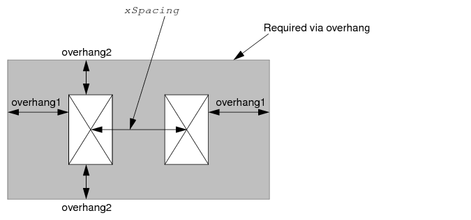
Example 1-45 Via Rule Generate Enclosure
The following example describes a formula for generating via cuts:
LAYER m1 ;
ENCLOSURE 0.05 0.01 ; #2 sides must be >=0.05, 2 other sides must be >=0.01
WIDTH 0.2 TO 100.0 ; #for m1, between 0.2 to 100 microns wide
LAYER m2 ;
ENCLOSURE 0.05 0.01 ; #2 sides must be >=0.05, 2 other sides must be >=0.01
WIDTH 0.2 TO 100.0 ; #for m2, between 0.2 to 100 microns wide
LAYER cut12
RECT -0.07 -0.07 0.07 0.07 ; #cut is .14 by .14
SPACING 0.30 BY 0.30 ; #center-to-center spacing
The cut layer SPACING ADJACENTCUTS statement can override the VIARULE cut layer SPACING statements. For example, assume the following cut layer information is also defined in the LEF file:
...
SPACING 0.20 ADJACENTCUTS 3 WITHIN 0.22 ;
...
The 0.20 μm edge-to-edge spacing in the ADJACENTCUTS statement is larger than the VIARULE GENERATE example spacing of 0.16 (0.30 − 0.14). Whenever the VIARULE GENERATE rule creates a via that is larger than 2x2 cuts (that is, 2x3, 3x2, 3x3 and so on), the 0.20 spacing from the ADJACENTCUTS statement is used instead.
Note: The spacing in VIARULE GENERATE is center-to-center spacing, whereas the spacing in ADJACENTCUTS is edge-to-edge.
|
LAYER cutLayerName |
||
|
LAYER routingLayerName |
||
|
Specifies the routing (or masterslice) layers for the top and bottom of the via. |
||
|
RECT pt pt |
||
|
Specifies the location of the lower left contact cut rectangle. |
||
|
RESISTANCE resistancePerCut |
||
|
Specifies the resistance of the cut layer, given as the resistance per contact cut. |
||
|
SPACING xSpacing BY ySpacing |
||
|
Note: This value can be overridden by the SPACING ADJACENTCUTS value in the cut layer statement. |
||
|
VIARULE viaRuleName |
||
|
Specifies the name for the rule. The name DEFAULT is reserved and should not be used for any via rule name. In the LEF and DEF VIA definitions that use generated via parameters, the reserved DEFAULT name indicates the via rule with the DEFAULT keyword. |
||
|
WIDTH minWidth TO maxWidth |
||
|
Specifies a wire width range to use for this VIARULE. This VIARULE can be used for wires with a width greater than or equal to (>=) minWidth, and less than or equal to (<=) maxWidth for the given routing (or masterslice) layer. If no WIDTH statement is specified, the VIARULE can be used for all wire widths on the given routing (or masterslice) layer. |
||