|
|
|||||||||
|
|
|
|
|
|
|
|
|
|
|
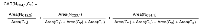
To determine the extent of the PAE, the router calculates the area of the layer relative to the area of the gates connected to it, or connected to it through lower layers. The number it calculates is called the antenna ratio. Each foundry sets a maximum allowable antenna ratio for the chips it fabricates.

To tell the router the values to use when it calculates the antenna ratio, you set antenna keywords in the LEF and DEF files. The router measures potential damage caused by PAE by checking the ratio it calculates against the values specified by the antenna keywords. When it finds a net whose antenna ratio for a specified layer exceeds the maximum allowed value for that layer, it finds a process antenna violation and attempts to fix it using one or both of the following methods:

|
Inserting diodes that protect the gate by providing an alternate path to discharge the static charge |
In a chip manufacturing process, metal layers are built up, layer by layer, starting with the first-level metal layer (usually referred to as metal1). Next, the metal1-metal2 vias are created, then the second-level metal layer, then metal2-metal3 vias, and so on.
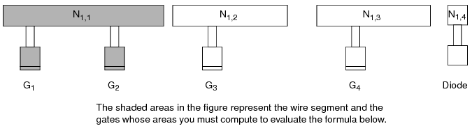
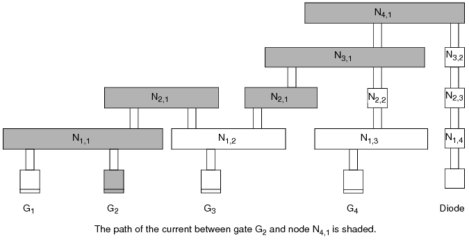
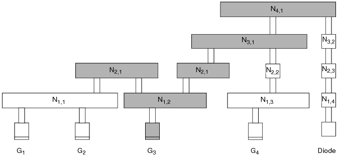
Figure C-1 shows a section of an imaginary chip after the unneeded metal from metal2 is removed.
|
|
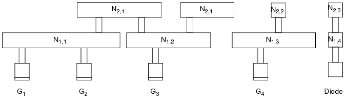
Gate areas for transistors are labelled Gk, where k is a sequential number starting with 1. |
|
|

|
N signifies that the wire segment is an electrically connected node |
|
|
|
i specifies the metal layer to which the node belongs |
|
|
|
j is a sequential number for the node on that metal layer |
|
|
Nodes are labelled so that all pieces of the metal geometry on layer metali that are electrically connected by conductors at layers below metali belong to the same node. For example, the two metal2 wire segments that belong to node N2,1 are electrically connected to gates G1, G2, and G3 by a piece of wire on metal1 (labelled N1,2). |
Thick oxide insulates the already-fabricated structures below metal2, preventing them from direct contact with the plasma. The metal2 geometries, however, are exposed to the plasma, and collect charge from it. As the metal geometries collect charge, they build up voltage potential.
In Figure C-1 , note the following:
|
|
Node N1,1 is electrically connected to gates G1 and G2. |
|
|
Node N1,2 is electrically connected to gate G3. |
|
|
Node N2,1 (node N2,1 has two pieces of metal) is electrically connected to gates G1, G2, and G3. |
|
|
Node N1,3 and node N2,2 are electrically connected to gate G4. |
|
|
Node N1,4 and node N2,3 are electrically connected to the diffusion (diode). |
In the imaginary chip in Figure C-1 , if the current were to flow, the following would happen, as a result of the node-gate connections:
|
|
The charge collected by process antennas on nodes N1,1, N1,2, and N2,1 would be discharged through one or more of gates G1, G2, and G3. |
|
|
The charge collected by process antennas on nodes N1,3 and N2,2 would be discharged through gate G4. |
|
|
The charge collected by process antennas on node N1,4 and N2,3 would be discharged through the diode. |
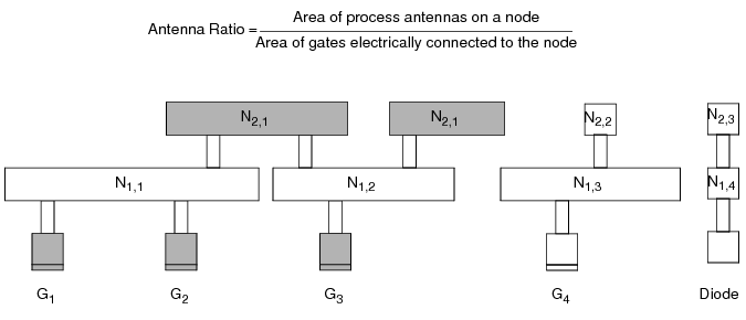
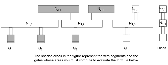
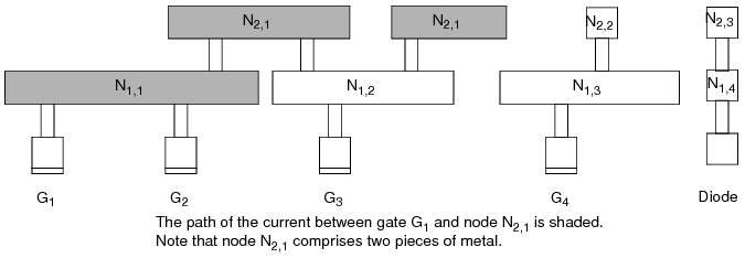
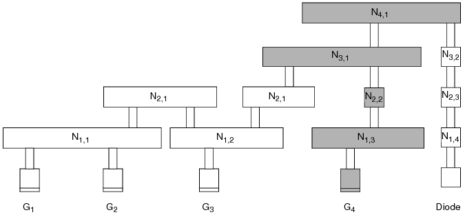
Figure C-2 shows the same section of the imaginary chip as the previous figure. The shaded areas in this figure represent the process antennas on node N2,1 and the gates to which they connect: gates G1, G2, and G3. The shaded gates discharge the electricity collected by the process antennas on node N2,1.
Routers typically use two methods to decrease the antenna ratio:
Both of these methods supply alternate paths for the current. For details about how to specify antenna diode cells, see "Using Antenna Diode Cells".
The following table lists LEF version 5.5 antenna keywords.
|
ANTENNAAREAFACTOR Note: Use DIFFUSEONLY if you want the multiplier to apply only when connecting to diffusion. For more information, see "Using DiffUseOnly". |
||
|
Relationship the router is calculating Cum is used in keywords for cumulative antenna ratio. |
Tools should calculate antenna ratios using one of the following models:
Using this model, you calculate damage to gates by process antennas on one layer. For example, if you use the partial checking model to calculate the PAE referred to a gate from metal3, you do not consider any potential damages referred to that gate from metallization steps on metal1 or metal2.
You use this model to calculate a partial antenna ratio (PAR). A PAR tells you if any single metallization step is likely to inflict damage to a gate.
This model is more conservative than the partial checking model. It adds damage to a gate caused by the PAE referred to the gate from each metallization step, starting from metal1 up to the layer that is being checked. For example, if you use the cumulative checking model to calculate the PAE referred to a gate from metal3, you add the PAR from the relevant antenna areas on metal1, metal2, and metal3.
You use this model to calculate a cumulative antenna ratio (CAR). A CAR adds the damages on successive layers together to accumulate them as the layers are built up.
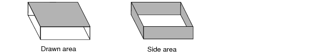
The area used to model the charge-collecting ability of a node is called the antenna area. The router calculates the antenna area for one of the following areas:
The height of each side is taken from the THICKNESS statement for that layer.
Figure C-3 shows drawn and side areas.
|
|
Use ANTENNAAREAFACTOR to adjust the calculation of the drawn area. |
|
|
Use ANTENNASIDEAREAFACTOR to adjust the calculation of the side area. |
The default value of both factors is 1.
The final ratio check can be scaled (that is, made more or less pessimistic) by using the ANTENNAAREAFACTOR or ANTENNASIDEAREAFACTOR values that are used to multiply the final PAR and CAR values.
Note: The LEF and DEF ANTENNA values are always unscaled values; only the final ratio-check is affected by the scale factors.
The general PAR(m1) equation for a single layer is calculated as:
The existing ANTENNAAREAFACTOR statement is shown as metalFactor for the metal area. It has no effect on the diff_area, gate_area, or cut_area shown. Likewise, the ANTENNAAREADIFFREDUCEPWL statement is shown as diffMetalReduceFactor, the ANTENNAAREAMINUSDIFF statement is shown as minusDiffFactor, and the ANTENNAGATEPLUSDIFF statement is shown as plusDiffFactor. For cut layer, the ratio equation illustrates the effect of an ANTENNAAREAFACTOR cutFactor statement as metalFactor. If there is no preceding ANTENNAAREAFACTOR statement, the metalFactor value defaults to 1.0.
For single layer rules, the PAR value is compared to ANTENNA[SIDE]AREARATIO and/or ANTENNADIFF[SIDE]AREARATIO, as appropriate. For cumulative layer rules, the CAR values is compared to ANTENNACUM[SIDE]AREARATIO and/or ANTENNACUMDIFF[SIDE]AREARATIO, as appropriate.

PAR(Ni,j, Gk) is the partial antenna ratio for node j on metali with respect to gate Gk, where Gk is electrically connected to node Ni,j by layer i or below.
Area(Ni,j) is the drawn or side area of node Ni,j.
C(Ni,j) is the set of gates Gk that are electrically connected to Ni,j through the layers below metali.
Area(Gk) is the drawn or side area of gate Gk. (The reason to include the Gk parameter for PAR is to maintain uniformity with the notation for CAR.)
Note: For a specified node Ni,j, the PAR(Ni,j, Gk) for all gates Gk that are connected to the node Ni,j using metali or below are identical.
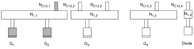
Figure C-4 shows a section of an imaginary chip after the first metal layer is processed.
To calculate PAR(Ni,j, Gk) for node N1,1, a node on the first metal layer, with respect to gate G1, use the following formula:

Because gates G1 and G2 both connect to node N1,1, the following statement is true:
To calculate PAR for node N1,2, another node on the first metal layer, with respect to gate G3, use the following formula:

To calculate PAR(Ni,j, Gk) for node N1,3, another node on the first metal layer, with respect to gate G4, use the following formula:

Figure C-5 shows the chip after the second metal layer is processed.
N2,1 consists of two pieces of metal on the second layer that are electrically connected at this step in the fabrication process. Therefore, to calculate PAR(N2,1,G1), you must add the area of both pieces together.
To calculate PAR(Ni,j,Gk) for node N2,1, a node on the second metal layer, with respect to gate G1, use the following formula:

PAR(N2,1,G1) = PAR(N2,1,G2) = PAR(N2,1,G3)
Figure C-6 shows the chip after the third metal layer is processed.
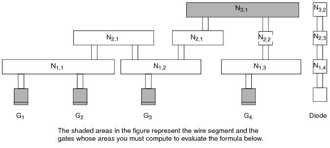
To calculate PAR(Ni,j, Gk)for node N3,1, a node on the third metal layer, with respect to gate G1, use the following formula:

PAR(N3,1,G1) = PAR(N3,1,G2) = PAR(N3,1,G3) = PAR(N3,1,G4)
Figure C-7 shows the chip after the fourth metal layer is processed.
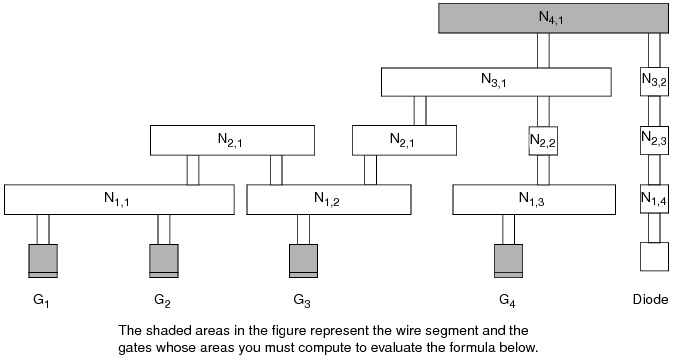
To calculate PAR(Ni,j, Gk) for the fourth metal layer, use the following formula:

PAR(N4,1,G1) = PAR(N4,1,G2) = PAR(N4,1,G3) = PAR(N4,1,G4)
Note: Node N4,1 is connected to the diffusion layer through the output diode. After the router calculates the antenna ratio, it compares its calculations to the area of the diffusion, instead of the area of the gates.
To calculate a CAR, the router adds the PARs for all the relevant nodes on the specified or lower metal layers that are electrically connected to a gate. Therefore, CAR(Ni,j,Gk) designates the cumulative damage to gate Gk by metallization steps up to the current level of metal, i.
To create a single accumulative model that combines both metal and cut damage into one model, specify the ANTENNACUMROUTINGPLUSCUT statement for the layer, so that:
CAR(mi) = PAR(mi) + CAR(vi-1)
Note: In practice, the router only needs to keep track of the worst-case CAR; however, the CARs for all of the gates shown in Figure C-8 are described here.
The router calculates an antenna ratio with respect to a node-gate pair. To find the CAR for the node Ni,j - gate Gk pair, you trace the path of the current between gate Gk and node Ni,j and add the PAR with respect to gate Gk for the all nodes in the path between the first metal layer and layer i that you can trace back to Gk.
|
|
|
In Figure C-8 , node N1,2 is not shaded because it was not electrically connected to G2 when metal1 was processed. That is, because the charge accumulated on N1,2 when metal1 was processed cannot damage gate G1, the router does not include it in the calculations for CAR(N2,1,G1). Another way to explain this is to say that the PAE from node N1,2 with respect to gate G2 is 0. |
Figure C-9 shows the chip after the first metal layer is processed.
CAR(N1,1,G1) = PAR(N1,1,G1)
CAR(N1,1,G2) = PAR(N1,1,G2)
Because PAR(N1,1,G1) equals PAR(N1,1,G2), CAR(N1,1,G1) equals CAR(N1,1,G2).
Note: In general, CAR(Ni,j,Gk) equals CAR(Ni,j,Gk') if the two gates Gk and Gk' are electrically connected to the same node on metal1, the lowest layer that is subject to the process antenna effect.
Figure C-10 shows the chip after the second metal layer is processed.
|
|
|
In the figure above, N1,2 is not included in the calculations for CAR(N2,1,G1) because it was not electrically connected to G1 when metal1 was processed. That is, because the charge accumulated on N1,2 when metal1 was processed cannot damage gate G1, the router does not include it in the calculations for CAR(N2,1,G1). |
CAR(N2,1,G1) = PAR(N1,1,G1) + PAR(N2,1,G1)
CAR(N2,1,G2) = PAR(N1,1,G2) + PAR(N2,1,G2)
Gates G1 and G2 have the same history with regard to PAE because they are connected to the same piece of metal1, so they have the same CAR for any node on a specified layer:
CAR(N2,1,G1) = CAR(N2,1,G2)
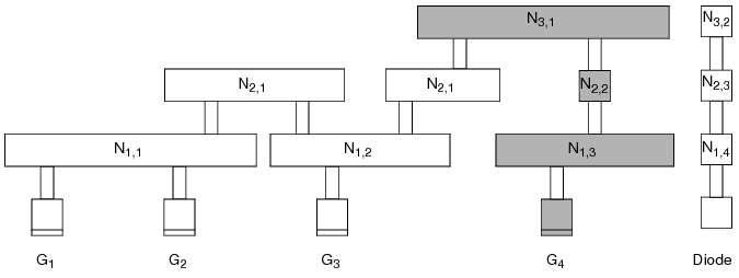
Figure C-11 shows the chip after the third metal layer is processed.
CAR(N3,1,G1) = PAR(N1,1,G1) + PAR(N2,1,G1) + PAR(N3,1,G1)
CAR(N3,1,G2) = PAR(N1,1,G2) + PAR(N2,1,G2) + PAR(N3,1,G2)
CAR(N3,1,G1) equals CAR(N3,1,G2) because gates G1 and G2 are both electrically connected to the same node, N1,1, on metal1 and therefore have the same history with regard to PAE. Therefore, the formula for CAR(N3,2, G2) is CAR(N3,1,G1) = CAR(N3,1,G2)
Gates G3 and G4 are not connected to the same node on metal1 and therefore do not have the same history with regard to PAE. Therefore, the CAR(N3,1,G3) and CAR(N3,1,G4) do not necessarily equal CAR(N3,1,G1) or CAR(N3,1,G2).
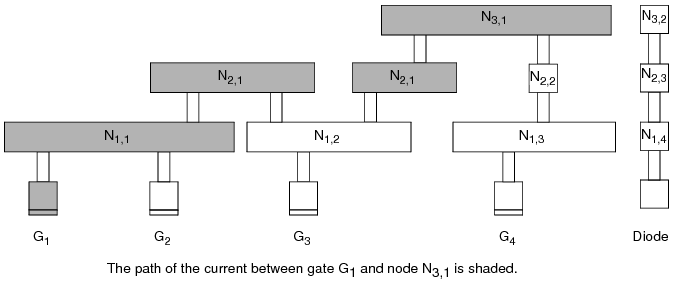
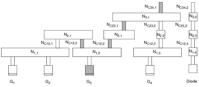
In Figure C-12 , the relevant areas for calculating CAR for gate G3 are shaded.
CAR(N3,1,G3) = PAR(N1,2,G3) + PAR(N2,1,G3) + PAR(N3,1,G3)
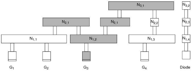
In Figure C-13 , the relevant areas for calculating CAR for gate G4 are shaded.
CAR(N3,1,G4) = PAR(N1,3,G4) + PAR(N2,2,G4) + PAR(N3,1,G4)
The following figure shows the chip after the fourth metal layer is processed.
Note: Node N4,1 is connected to the diffusion layer through the output diode. After the router calculates the antenna ratio, it compares its calculations to the area of the diffusion, instead of the area of the gates.
In Figure C-14 , the relevant areas for calculating CAR(N4,1,G1) and CAR(N4,1,G2) are shaded.
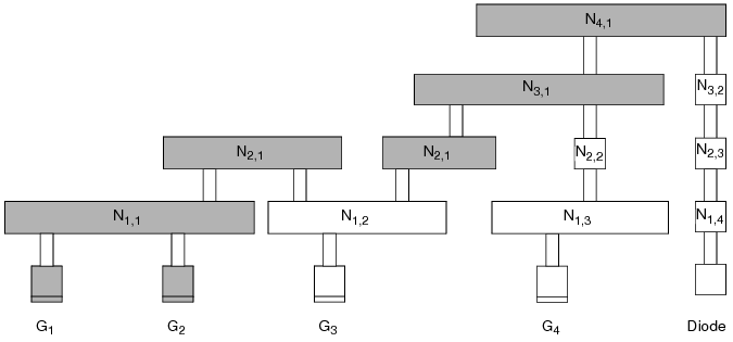
CAR(N4,1,G1) = PAR(N1,1,G1) + PAR(N2,1,G1)
+ PAR(N3,1,G1) + PAR(N4,1,G1)
CAR(N4,1,G2) = PAR(N1,1,G2) + PAR(N2,1,G2)
+ PAR(N3,1,G2) + PAR(N4,1,G2)
CAR(N4,1,G1) = CAR(N4,1,G2)
In Figure C-15 , the relevant areas for calculating CAR(N4,1,G3) are shaded.
CAR(N4,1,G3) = PAR(N1,2,G3) + PAR(N2,1,G3)
+ PAR(N3,1,G3) + PAR(N4,1,G3)
CAR(N4,1,G3) does not equal CAR(N4,1,G1) or CAR(N4,1,G2) because it is not connected to the same node on metal1.
In Figure C-16 , the relevant areas for calculating CAR(N4,1,G4) are shaded.
CAR(N4,1,G4) = PAR(N1,3,G4) + PAR(N2,2,G4)
+ PAR(N3,1,G4) + PAR(N4,1,G4)
CAR(N4,1,G4) does not equal CAR(N4,1,G1), CAR(N4,1,G2), or CAR(N4,1,G3) because it is not connected to the same node on metal1.
The general PAR(ci) equation for a single layer is calculated as: 
The existing ANTENNAAREAFACTOR statement is shown as cutFactor for the metal area. Likewise, the ANTENNAAREADIFFREDUCEPWL statement is shown as diffAreaReduceFactor, the ANTENNAAREAMINUSDIFF statement is shown as minusDiffFactor, and the ANTENNAGATEPLUSDIFF statement is shown as plusDiffFactor. For cut layer, the ratio equation illustrates the effect of an ANTENNAAREAFACTOR cutFactor statement as metalFactor. If there is no preceding ANTENNAAREAFACTOR statement, the metalFactor value defaults to 1.0.
In the figures and text that follow,
|
|
Cij is the cut layer between metali and metalj. |
|
|
NCij,k specifies an electrically connected node on Cij. |
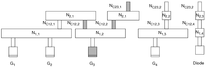
Figure C-17 shows the chip after the C12 process step.

As in calculations on the metal layers,
PAR(NC12,1,G1) = PAR(NC12,1,G2)
As explained in "Calculating Antenna Ratios":
CAR(ci) = PAR(ci) + CAR(ci-1)
To create a single accumulative model that combines both metal and cut damage into one model, specify the ANTENNACUMROUTINGPLUSCUT statement for the layer, so that:
CAR(ci) = PAR(ci) + CAR(mi-1)
This means that the CAR from the metal layer below this cut layer is accumulated, instead of the CAR from the cut layer below this cut layer.
Figure C-18 shows the chip after the C23 process step.
The router calculates the CAR with respect to gate G3 after the cut C23 process step as follows:

Figure C-19 shows the chip after the C34 process step.
The router calculates the CAR with respect to gate G3 after the cut C34 process step as follows:
The area ratio check compares the PAR for each layer to the value of the ANTENNAAREARATIO or ANTENNADIFFAREARATIO.
The router calculates the PAR as follows:

According to the formula above, the area ratio check finds the PAR for node Ni,j with respect to gate Gk by dividing the drawn area of the node by the area of the gates that are electrically connected to it. The final PAR is multiplied by the ANTENNAAREAFACTOR (the default value for the factor is 1) and compared to the ANTENNAAREARATIO or ANTENNADIFFAREARATIO. If the PAR is greater than the ANTENNAAREARATIO or ANTENNADIFFAREARATIO specified in the LEF file, the router finds a process antenna violation and attempts to fix it.
The link between PAR(Ni,j,Gk) and a PAE violation at node Ni,j depends on whether node Ni,j is connected to a piece of diffusion, as follows:
|
|
If there is no connection from node Ni,j to a diffusion area through the current and lower layers, a violation occurs when the PAR is greater than the ANTENNAAREARATIO. |
|
|
If there is a connection from node Ni,j to a diffusion area through current and lower layers, a violation occurs when the PAR is greater than the ANTENNADIFFAREARATIO. |
|
|
If there is a connection from node Ni,j to a diffusion area through current and lower layers, and ANTENNADIFFAREA is not specified for an output or inout pin, the value is 0. |
The side area ratio check compares the PAR computed based on the side area of the nodes for each layer to the value of the ANTENNASIDEAREARATIO or ANTENNADIFFSIDEAREARATIO.
The router calculates the PAR as follows:

According to the formula above, the area ratio check finds the PAR for node Ni,j with respect to gate Gk by dividing the side area of the node by the area of the gates that are electrically connected to Ni,j. The final PAR is multiplied by the ANTENNASIDEAREAFACTOR (the default value for the factor is 1) and compared to the ANTENNASIDEAREARATIO or ANTENNADIFFSIDEAREARATIO. If the PAR is greater than the ANTENNASIDEAREARATIO or ANTENNADIFFSIDEAREARATIO specified in the LEF file, the router finds a process antenna violation and attempts to fix it.
The link between PAR(Ni,j,Gk) and a PAE violation at node Ni,j depends on whether node Ni,j is connected to a piece of diffusion, as follows:
|
|
If there is no connection to the diffusion area through the current and lower layers, a violation occurs when the PAR is greater than the ANTENNASIDEAREARATIO. |
|
|
If there is a connection to the diffusion area through current and lower layers, a violation occurs when the PAR is greater than the ANTENNADIFFSIDEAREARATIO. |
|
|
If there is a connection to the diffusion area through current and lower layers, and ANTENNADIFFAREA is not specified for an output or inout pin, the value is 0. |
The cumulative area ratio check compares the CAR to the value of ANTENNACUMAREARATIO or ANTENNACUMDIFFAREARATIO. The CAR is equal to the sum of the PARs of all nodes on the same or lower layers that are electrically connected to the gate.
Note: When you use CARs, you can ignore metal layers by not specifying the CAR keywords for those layers. For example, if you want to check metal1 using a PAR and the remaining metal layers using a CAR, you can define ANTENNAAREARATIO or ANTENNASIDEAREARATIO for metal1, and ANTENNACUMAREARATIO or ANTENNACUMSIDEAREARATIO for the remaining metal layers.
The cumulative area ratio check finds the CAR for node Ni,j with respect to gate Gk by adding the PARs for all layers of metal, from the current layer down to metal1, for all nodes that are electrically connected Gk. The final CAR is multiplied by the ANTENNAAREAFACTOR (the default value for the factor is 1) and compared to the ANTENNACUMAREARATIO or ANTENNACUMDIFFAREARATIO. If the CAR is greater than the ANTENNACUMAREARATIO or ANTENNACUMDIFFAREARATIO specified in the LEF file, the router finds a process antenna violation and attempts to fix it.
The link between CAR(Ni,j,Gk) and a PAE violation at node Ni,j depends on whether node Ni,j is connected to a piece of diffusion, as follows:
|
|
If there is no connection to a diffusion area through the current and lower layers, a violation occurs when the CAR is greater than the ANTENNACUMAREARATIO. |
|
|
If there is a connection to a diffusion area through current and lower layers, a violation occurs when the CAR is greater than the ANTENNACUMDIFFAREARATIO. |
|
|
If there is a connection to a diffusion area through current and lower layers, and ANTENNADIFFAREA is not specified for an output or inout pin, the value is 0. |
The cumulative side area ratio check compares the CAR to the value of the ANTENNACUMSIDEAREARATIO or ANTENNACUMDIFFAREARATIO.
Note: When you use CARs, you can ignore metal layers by not specifying the CAR keywords for those layers. For example, if you want to check metal1 using a PAR and the remaining metal layers using a CAR, you can define ANTENNAAREARATIO or ANTENNASIDEAREARATIO for metal1, and ANTENNACUMAREARATIO or ANTENNACUMSIDEAREARATIO for the remaining metal layers.
The cumulative side area ratio check finds the CAR for node Ni,j with respect to gate Gk by adding the PARs for all layers of metal, from the current layer down to metal1, for all nodes that are electrically connected Gk. The final CAR is multiplied by the ANTENNASIDEAREAFACTOR (the default value for the factor is 1) and compared to the ANTENNACUMSIDEAREARATIO or ANTENNACUMDIFFAREARATIO. If the CAR is greater than the ANTENNACUMSIDEAREARATIO or ANTENNACUMDIFFAREARATIO specified in the LEF file, the router finds a process antenna violation and attempts to fix it.
|
|
If there is no connection to a diffusion area through the current and lower layers, a violation occurs when the CAR is greater than the ANTENNACUMSIDEAREARATIO. |
|
|
If there is a connection to a diffusion area through current and lower layers, a violation occurs when the CAR is greater than the ANTENNACUMSIDEAREARATIO. |
|
|
If there is a connection to a diffusion area through current and lower layers, and ANTENNACUMDIFFAREA is not specified for an output or inout pin, the value is 0. |
To create the following process antenna rule for a cut layer via1:
cut_area / (gate_area + 2.0 x diff_area) <= 10
Cut layers should include the following information:
ANTENNAGATEPLUSDIFF 2.0 ;
ANTENNADIFFAREARATIO 10 ;
Assume the following process antenna rule:
cut_area x PWL(diff_area) / gate_area <= 10
This rule uses a cumulative model with diffusion area reduction function, where:
|
|
|
diffReduceFactor = 1.0 for diff_area < 0.1μm2 |
|
|
|
diffReduceFactor = 0.2 for diff_area >= 0.1 μm2 |
Cut layers should include the following information:
ANTENNAAREADIFFREDUCEPWL ( ( 0.0 1.0 ) ( 0.0999 1.0 ) ( 0.1 0.2 )
( 1000.0 0.2 ) ) ;
ANTENNACUMDIFFAREARATIO 10 ;
For examples of models that use the ANTENNACUMROUTINGPLUSCUT and the ANTENNAAREAMINUSDIFF rules, see the examples below in "Routing Layer Process Antenna Models."
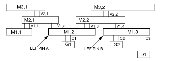
The following process antenna rule examples use the topology shown in Figure C-20. In this figure, there are two polysilicon gates (G1, G2), one diffusion connection (D1), contacts (C), and via (V1, V2) and metal (M1, M2, M3) shapes. Note that M1,2 is one LEF PIN, and M1,3 is a different LEF PIN. The other metal is routing.
Figure C-20
The following area values are also used for the examples:
The following process antenna rule combines cut area and metal area into one cumulative rule:
ratio = (metal _area + 10 x cut_area) / gate_area
Every routing layer should include the following information:
ANTENNACUMDIFFAREARATIO ( ( 0.0 1000 ) ( 0.0999 1000 ) ( 0.1 4000 )
( 1000.0 4000 ) ) ;
ANTENNADIFFAREARATIO ( ( 0.0 5000 ) ( 0.0999 500 ) ( 0.1 1500 )
( 1000.0 1500 ) ) ;
Every cut layer should include the following information:
ANTENNAAREAFACTOR 10 ; #10.0 x cut area
ANTENNACUMDIFFAREARATIO ( ( 0.0 1000 ) ( 0.0999 1000 ) ( 0.1 4000 )
( 1000.0 4000 ) ) ;
ANTENNADIFFAREARATIO ( ( 0.0 5000 ) ( 0.0999 500 ) ( 0.1 1500 )
( 1000.0 1500 ) ) ;
Note: ANTENNAAREARATIO and ANTENNACUMAREARATIO are not required because the *DIFFAREARATIO statements are checked, even if diff_area is equal to 0.
For gate G1, the PARs and CARs are computed as follows:
The polysilicon and contact cut layer and shapes are not normally visible in LEF and DEF. If the contact cut area should be included, its CAR value should be included with LEF PIN A, using appropriate ANTENNA statements. The M1 PIN area should not be included because M1 area is a PIN shape in the LEF and will be added in by tools reading LEF. Therefore, there should be two antenna statements for LEF PIN A, either:
ANTENNAGATEAREA 1.0 LAYER M1 ;
ANTENNAMAXCUTCAR 1.0 LAYER C ;
or:
ANTENNAGATEAREA 1.0 LAYER M1 ;
ANTENNAMAXAREACAR 1.0 LAYER M1 ;
Because the M1 PIN area is not included in the MAXAREACAR value, both of sets of statements give the same results. For more details, see "Calculations for Hierarchical Designs."
Similarly, the LEF PIN B should have values, such as either:
ANTENNAGATEAREA 2.0 LAYER M1 ;
ANTENNADIFFAREA 0.5 LAYER M1 ;
ANTENNAMAXCUTCAR 1.0 LAYER C ; #only C2 affects G2; C3 does not
or:
ANTENNAGATEAREA 2.0 LAYER M1 ;
ANTENNADIFFAREA 0.5 LAYER M1 ;
ANTENNAMAXAREACAR 1.0 LAYER M1 ; #only C2 affects G2; C3 does not
|
|
diode_area = 0, single-layer PWL(0) = 500, check PAR(M1,G1) = 2.0 <= 500, cum-layer PWL(0) = 1000, therefore check CAR(M1,G1) = 3.0 <= 1000 |
|
|
diode_area = 0, single-layer PWL(0) = 500, check PAR(V1,G1) = 2.0 <= 500, cum_layer PWL(0) = 1000, therefore check CAR(V1,G1) = 5.0 <= 1000 |
|
|
diode_area = 0.5, single-layer PWL(0.5) = 1500, check PAR(M2,G1) = 3.0 <= 1500, cum_layer PWL(0.5) = 4000, therefore check CAR(M2, G1) = 8.0 <= 4000 |
|
|
diode_area = 0.5, single-layer PWL(0.5) = 1500, check PAR(V2,G1) = 0.67 <= 1500, cum_layer PWL(0.5) = 4000, therefore check CAR(V2, G1) = 8.67 <= 4000 |
|
|
diode_area = 0.5, single-layer PWL(0.5) = 1500, check PAR(M3,G1) = 5 <= 1500, cum_layer PWL(0.5) = 4000, therefore check CAR(M3,G1) = 13.67 <= 4000 |
ratio = [(metal_area + 10 x cut_area) - (100 x diff_area)] / gate_area
Every routing layer should include the following information:
ANTENNACUMDIFFAREARATIO 1000 ;
Every cut layer should include the following information:
ANTENNAAREAFACTOR 10 ; #10.0 x cut area
ANTENNACUMDIFFAREARATIO 1000 ;
For gate G1, the PARs and CARs are computed as follows:
This value is on the LEF PIN, as mentioned in Example 1.
|
|
CAR(M1,G1) = PAR(M1,G1) + PIN A's CAR(C,G1) PIN A's CAR(M1) = ANTENNAMAXAREACAR for LAYER M1 = 1.0 = 2.0 + 1.0 = 3.0 |
|
|
Check CAR(M1,G1) = 3.0 <= 1000 |
|
|
PAR(V1,G1) = [10 x area(V1,2 + V1,3) - (100 x diff_area)] / area(G1) = [(10 x .2) - (100 x 0)] / (1) = 2.0 |
|
|
Check CAR(V1,G1) = 5.0 <= 1000 |
|
|
PAR(M2,G1) = [area(M2,1 + M2,2) - (100 x area(D1))] / area(G1 + G2) = [(4 + 5) - (100 x 0.5) / (1 + 2) = -13.67 |
|
|
CAR(M2,G1) = PAR(M2,G1) + CAR(V1,G1) = -13.67 + 5.0 = -8.67, truncate to 0 |
|
|
Check CAR(M2,G1) = 0 <= 1000 |
|
|
PAR(V2,G1) = [(10 x area(V2,1 + V2,2)) - (100 x area(D1)] / area(G1 + G2) = [(10 x 0.2) - (100 x 0.5)] / (1 + 2) = -16.0 |
|
|
CAR(V2,G1) = PAR(V2,G1) + CAR(M2,G1) = -16.0 + 0 = -16.0, truncate to 0 |
|
|
Check CAR(V2,G1) = 0 <= 1000 |
|
|
PAR(M3,G1) = [area(M3,1 + M3,2) - (100 x area(D1))] / area(G1 + G2) = [(6 + 9) - (100 x 0.5)] / (1 + 2) = -11.67 |
|
|
Check CAR(M3,G1) = 0 <= 1000 |
Single layer: metal_area / (gate_area + 2.0 x diff_area) <= 1000
Cumulative for the layer: metal_area / (gate_area + 2.0 x diff_area) <= 5000
Every metal layer should include the following information:
ANTENNACUMDIFFAREARATIO 5000 ;
For gate G1, the PARs and CARs are computed as follows:
|
|
Check PAR(M1,G1) = 2 <= 1000, check CAR(M1,G1) = 2 <= 5000 |
|
|
Check PAR(M1,G1) = 2.25 <= 1000, check CAR(M1,G1) = 4.25 <= 5000 |
|
|
Check PAR(M1,G1) = 3.75 <= 1000, check CAR(M1,G1) = 8.0 <= 5000 |
Every metal layer should include the following information:
ANTENNAAREADIFFREDUCEPWL ( ( 0.0 1.0 ) ( 0.0999 1.0 ) ( 0.1 0.2 )( 1.0 0.1 )
( 1000.0 0.1 ) ) ;" ;
ANTENNACUMDIFFAREARATIO 1000 ;
For gate G1, the PARs and CARs are computed as follows:
|
|
Initial PAR(M1,G1) = area(M1,2) / area(G1) = 2.0 / 1 = 2 |
|
|
diode_area = 0, PWL(0) = 1.0, therefore initial PAR(M1,G1) is multiplied by 1.0 to give PAR(M1,G1) = 2 x 1 = 2 |
|
|
Check CAR(M1,G1) <= 1000, therefore check 2 <= 1000 |
|
|
Initial PAR(M2,G1) = area(M2,1 + M2,2) / area(G1 + G2) = (4 + 5) / (1 + 2) = 3 |
|
|
diode_area = 0.5, PWL(0.5) = 0.155, therefore initial PAR(M2,G1) is multiplied by 1.0 to give PAR(M2,G1) = 3 x 0.155 = 0.465 |
|
|
Check CAR(M2,G1) <= 1000, therefore check 2.465 <= 1000 |
|
|
Initial PAR(M3,G1) = area(M3,1 + M3,2) / area(G1 + G2) = (6 + 9) / (1 + 2) = 5 |
|
|
Check CAR(M3,G1) <= 1000, therefore check 3.24 <= 1000 |
Assume you have the following antenna rules for your process:
The corresponding LEF file would include:
ANTENNACUMAREARATIO 1000 ;
PWL ( ( 0 1000 ) ( 0.099 1000 ) ( 0.1 5200 ) ( 100 205000 ) ) ;
PWL ( ( 0 20 ) ( 0.099 20 ) ( 0.1 120 ) ( 100 20100 ) ) ;
A typical standard cell that has only M1 pins and routing inside of it would have:
ANTENNAGATEAREA .5 LAYER M1 ; # connects to 0.5 μm^2 poly gate
ANTENNAPARTIALMETALAREA 1.0 LAYER M1 ; # has 1.0 μm^2 M1 area.
# Note that it should not include the M1 pin area, just the M1 routing
# area that is not included in the PIN shapes. In many cases, all of the
# M1 routing is included in the PIN, so this value is 0, and not in the
ANTENNAMAXAREACAR 10.0 LAYER M1 ; # has 10.0 cumulative ratio so far.
# This value can include area from internal poly routing if poly routing
# damage is accumulated with the metal layers. It does not include
# the area of the M1 pin area, just the M1 routing area that is not
# included in the PIN shapes. If poly damage is not included, and all
# of the M1 routing is included in the PIN, this value will be 0, and
ANTENNADIFFAREA .2 LAYER M1 ; # connects to 0.2 μm^2 difusion area
ANTENNAPARTIALMETALAREA 1.0 LAYER M1 ; # has 1.0 μm^2 M1 area
# No ANTENNAMAXAREACAR value because no internal poly gate is connected
Routers generally use one of two methods to fix process antenna violations:
The following example shows a LEF definition of an antenna diode cell, with the CLASS CORE ANTENNACELL and ANTENNADIFFAREA defined:
RECT 0.190 2.380 0.470 2.660 ;
LEF defines only one value for ANTENNAAREAFACTOR and one value for ANTENNASIDEAREAFACTOR, with or without DIFFUSEONLY, per layer. If you specify more than one antenna area or side area factor for a layer, only the last one is used. The AREAFACTOR value lets you scale the value of the metal area. If you use the DIFFUSEONLY keyword, only metal attached to diffusion is scaled.
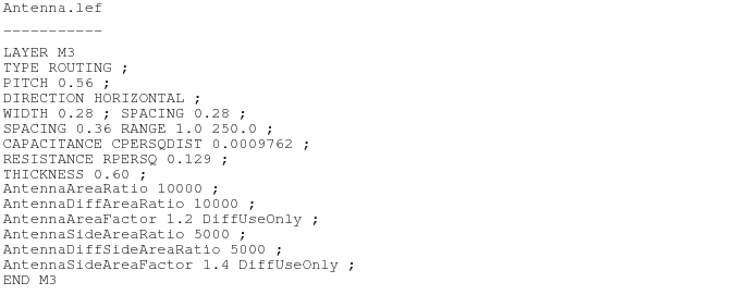
Suppose you have the following LEF file:
|
|
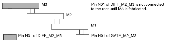
The input pin H01 of GATE_M2_M3 connects the metal wires to metal1, metal2, and metal3 in sequence. |
|
|
The ANTENNAAREAFACTOR 1.2 DIFFUSEONLY and ANTENNASIDEAREAFACTOR 1.4 DIFFUSEONLY apply to metal3 routing. |
|
|
Prior to metal3 fabrication, there is no path to the diffusion diode. This causes the default factor of 1.0 to apply to the metal1 and metal2 segments shown when calculating PARs. |
The following section illustrates computation of antenna ratios for hierarchical designs.
|
Drawn area or side area of the metal wires. Measured in square microns. |
||
|
Relationship the router is calculating CAR is used in keywords for cumulative antenna ratio. |
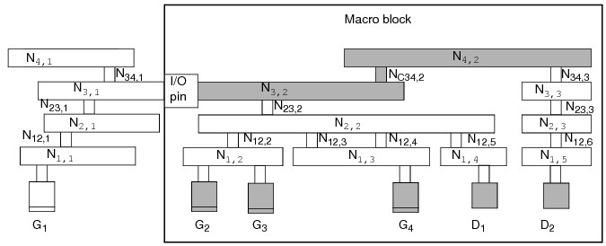
Figure C-22 represents a macro block. This block can be a custom hard block or part of a bottom-up hierarchical flow. The resulting PAE values will be the same in either case. In the example,
|
|
Gates G1, G2, G3, and G4 are the same size. |
|
|
Node N1,3 is larger than node N1,2. |
|
|
The I/O pin is on metal3. |
|
|
The area of diffusion for D1 is area(Diff1). |
|
|
The area of diffusion for D2 is area(Diff2). |
|
|
The area of the cut layer that connects node N3,1 and node N4,2 is area(NC34,1). |
ANTENNAPARTIALMETALAREA area(N3,2) LAYER Metal3 ;
ANTENNAPARTIALMETALAREA area(N4,2) LAYER Metal4 ;
ANTENNAPARTIALMETALSIDEAREA sideArea(N3,2) LAYER Metal3 ;
ANTENNAPARTIALMETALSIDEAREA sideArea(N4,2) LAYER Metal4 ;
You do not need to specify an ANTENNAPARTIALMETALAREA or ANTENNAPARTIALSIDEMETALAREA for any layer lower than metal3 because the I/O pin is on metal3; that is, there is no connection outside the block until metal3 is processed.
ANTENNAGATEAREA area(G2 + G3 + G4) LAYER Metal3 ;
ANTENNADIFFAREA area(Diff1) LAYER Metal3 ;
ANTENNADIFFAREA area(Diff1 + Diff2) LAYER Metal4 ;
ANTENNAPARTIALCUTAREA area(N34,2) LAYER Via34 ;
Use the following keywords to calculate the actual CAR on the I/O pin layer or above.
For the example in Figure C-22 , the keywords and calculations for metal3 and via34 would be:
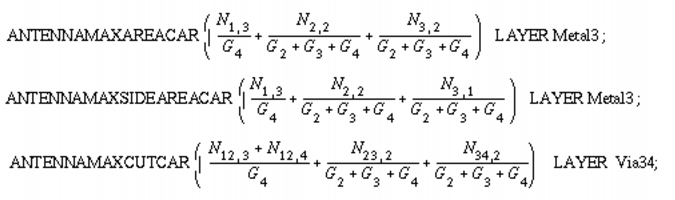
For a macro block like that shown in Figure C-22 , you should have the following pin information in your LEF file, ignoring SIDEAREA values:
ANTENNAGATEAREA 0.3 LAYER METAL3 ; # area of G2 + G3 + G4
ANTENNADIFFAREA 1.0 LAYER METAL3 ; # area of D1
ANTENNAPARTIALMETALAREA 10.0 LAYER METAL3 ; # area of N3,2
ANTENNAMAXAREACAR 100.0 LAYER METAL3 ; # max CAR of N3,2
ANTENNAPARTIALCUTAREA 0.1 LAYER VIA34 ; # area of N34,2
ANTENNAMAXCUTCAR 5.0 LAYER VIA34 ; # max cut CAR of N34,2
ANTENNAGATEAREA 0.3 LAYER METAL4 ; # area of G2 + G3 + G4
ANTENNADIFFAREA 2.0 LAYER METAL4 ; # area of D1 + D2
ANTENNAPARTIALMETALAREA 12.0 LAYER METAL4 ; # area of N4,2
ANTENNAMAXAREACAR 130.0 LAYER METAL4 ; # max CAR of N4,2
MACRO macroName
CLASS BLOCK ;
PIN pinName
DIRECTION OUTPUT ;
[ANTENNAPINPARTIALMETALAREA value [LAYER layerName] ;] ...
[ANTENNAPINPARTIALMETALSIDEAREA value [LAYER layerName] ;] ...
[ANTENNAPINGATEAREA value [LAYER layerName] ;] ...
[ANTENNAPINDIFFAREA value [LAYER layerName] ;] ...
[ANTENNAPINMAXAREACAR value [LAYER layerName] ;] ...
[ANTENNAPINMAXSIDEAREACAR value [LAYER layerName] ;] ...
[ANTENNAPINPARTIALCUTAREA value [LAYER cutlayerName] ;] ...
[ANTENNAPINMAXCUTCAR value LAYER cutlayerName] ;] ...
END Z
END macroName
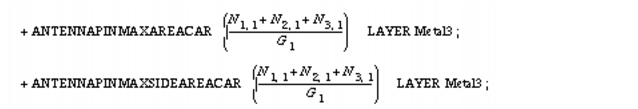
An example of the DEF keywords for Figure C-22 would be:
- example + NET example1
+ ANTENNAPINPARTIALMETALAREA (N3,1) LAYER Metal3 ;
+ ANTENNAPINPARTIALMETALSIDEAREA (N3,1) LAYER Metal3 ;
+ ANTENNAPINGATEAREA (G1) LAYER Metal3 ;
# No ANTENNAPINDIFFAREA for this example
+ ANTENNAPINPARTIALCUTAREA (N34,1) LAYER via34 ;
+ ANTENNAPINGATEAREA (G1) LAYER Metal4 ;
+ ANTENNAPINPARTIALMETALAREA (N4,1) LAYER Metal4 ;
+ ANTENNAPINPARTIALMETALSIDEAREA (N4,1) LAYER Metal4 ;
...