Draw a Stack of Transistors. More...
Inherits object.
Public Member Functions | |
| def | __init__ (self, device, NERC, NIRC) |
| [API] Constructor More... | |
| def | setWirings (self, wiringSpec) |
| [API] Set the Stack wiring specification. More... | |
| def | computeDimensions (self) |
| [internal] Compute Stack dimensions from the technological rules. More... | |
| def | doLayout (self, bbMode) |
| [API] Draw the complete layout. More... | |
Detailed Description
Draw a Stack of Transistors.
A Stack of Transistors is a set of transistor put into a regular band and connected through their sources/drains. All share the exact same W & L. The way they are connecteds defines what functionnality the Stack implement.
The abutment box of the stack is adjusted so that both height and width are even multiples of the track pitches, so the device can be easily placed and handled by the mixed router. The extra space needed for padding is added around the active area. Due to the presence of tracks at the top and bottom of the stack, the active area will be horizontally centered but not vertically.
The drawing of the stack is controlled through a set of variables (attributes) that allows to create it regardless of the technology. The technology is taken into account in the way those variables are computed and, obviously, their values. The following schematics details the main stack drawing variables along with their computations.
Stack Layout
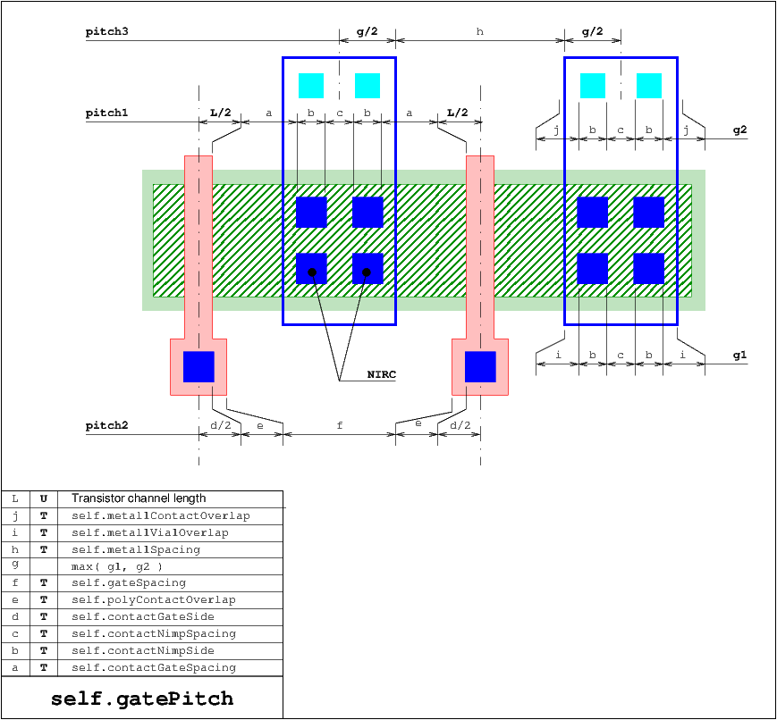
Gate pitch
self.gatePitch: the pitch of transistors gates, inside the stack. It also applies to dummy transistors.
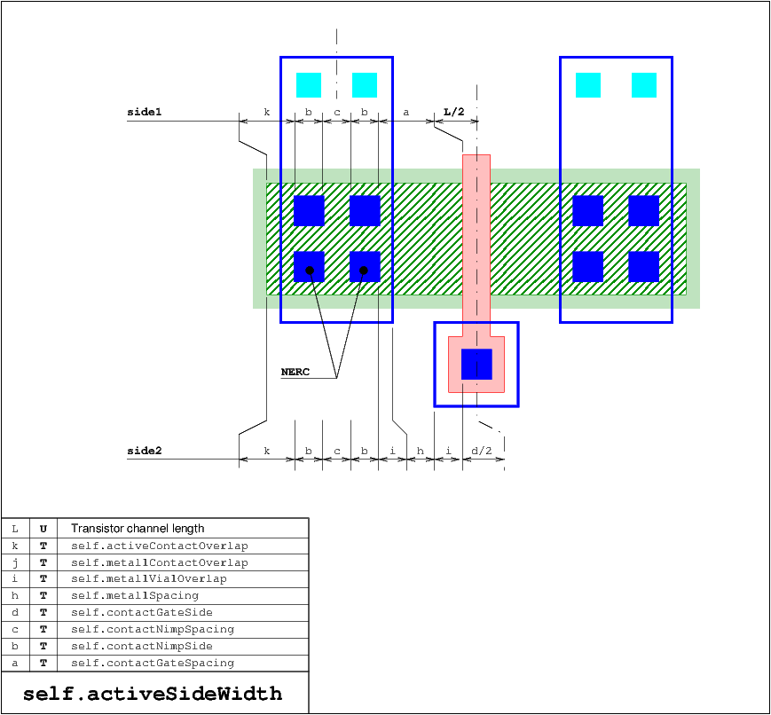
Active Side Width
self.activeSideWidth: the distance between the axis of the last transistor gate (on the left or right) and the edge of the active area (not the diffusion area).
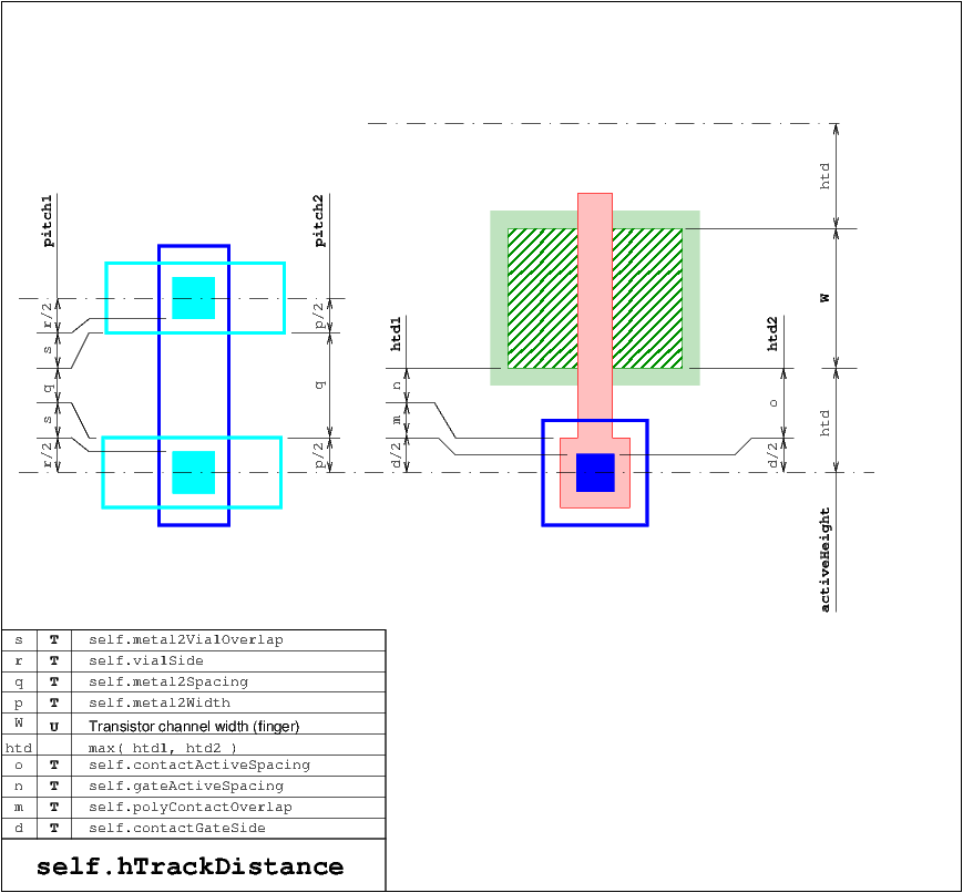
H-Track Distance
self.hTrackDistance: the minimal distance between either the top or bottom edge of the active area and the axis of the first track.
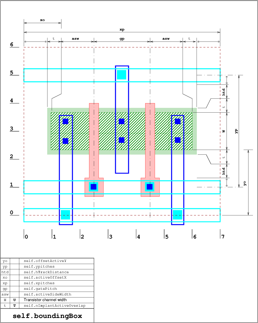
BoundingBox & Overall Variables
self.xpitches: the number of vertical track pitches needed to fully enclose the active area.self.ypitches: the number of horizontal track pitches needed to fully enclose the active area.self.activeOffsetX&self.activeOffsetY: the offsets of the active area from the bottom left corner of the abutment box.self.diffusionWidth&self.diffusionHeightare the minimun dimensions required to fit the active area.self.topTracksNb(): the number of tracks at the top of the stack.self.botTracksNb(): the number of tracks at the bottom of the stack.
Wiring Specifications
Stack routing is done through vertical metal1 wires coming from the gates and diffusions areas and metal2 horizontal wires that can be either above or below the active area. metal2 wires (or track) goes through the whole stack and are assigned to one net only. A net will have at least one track above or below and may have both.
The connections to the diffusions areas and gates of the various fingers are specified through a list. The stack is made of a regular alternation of diffusions and gates. The list tells, for each one starting from the left, to which net and track they are connected. For a stack of  transistor fingers, the must wiring specification must contains
 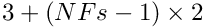 elements. The list is given through one string with each elements separated by one or more whitespace. The syntax for one element is detailed Atomic Wiring Specification.
Track numbering scheme
Tracks above (top) the active area and below (bottom) each have their own numbering. In both case, the count start from the active area. This, the top tracks will be numbered by increasing Y and the bottom tracks by decreasing Y.
Track/Net assignement
The track/net assignement is deduced from the atomic wiring specifications. It also allows to compute the total number of tracks needed above and below the active area.
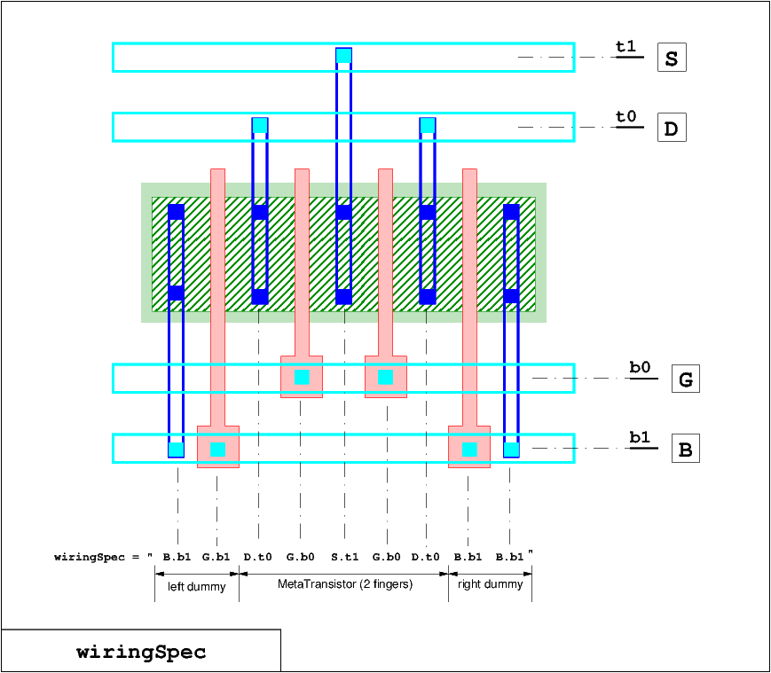
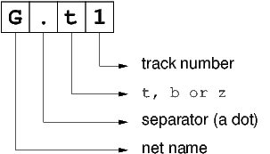
Atomic Wiring Specification
An atomic wiring specification has the same syntax for either diffusions or gates. It must not comprise any whitespaces. it is made of the following parts:
- The net name to connect to.
- Whether the track is above the active area (
"t") or below ("b"). The special case ("z") means that this element must be left unconnected (is such case possible?). - The number of the track.
Stack Implementation Details
The __setattr__() and __getattr__ functions have been redefined so that the technological values (rules) can be accessed has normal attributes of the Stack class, in addition to the regular ones.
Constructor & Destructor Documentation
◆ __init__()
| def __init__ | ( | self, | |
| device, | |||
| NERC, | |||
| NIRC | |||
| ) |
[API] Constructor
param rules The physical rule set.
- Parameters
-
device The Hurricane AMS device into which the layout will be drawn. NERC Number of contact rows in external (first & last) diffusion connectors. NIRC Number of contact rows in middle diffusion connectors. param w The width of every transistor of the stack (aka fingers). param L The length of every transistor. param NFs The total number of fingers (dummies includeds). param NDs The number of dummies to put on each side of the stack.
References Stack.bImplantLayer, Stack.botTracks, Stack.botWTracks, Stack.bulkNet, Stack.bulks, CapacitorStack.device, CapacitorUnit.device, VerticalRoutingTracks.device, Stack.device, Stack.dimensioned, Bulk.flags, Stack.flags, Stack.isNmos(), Stack.L, Stack.metaTnb(), Stack.metaTransistors, Stack.NDs, Stack.NERC, Stack.NFs, Stack.NIRC, Stack.tImplantLayer, Stack.topTracks, Stack.topWTracks, Stack.w, Stack.wellLayer, and Stack.wirings.
Member Function Documentation
◆ setWirings()
| def setWirings | ( | self, | |
| wiringSpec | |||
| ) |
[API] Set the Stack wiring specification.
- Parameters
-
wiringSpec A string defining the connections for the gates and diffusion areas.
For a comprehensive explanation of the wiring specification, refers to Wiring Specifications .
References Stack.botTracks, Stack.botTracksNb(), Stack.botWTracks, Stack.bulkNet, Stack.computeDimensions(), RoutMatchedCapacitor.computeDimensions(), CapacitorUnit.computeDimensions(), CapacitorStack.device, CapacitorUnit.device, VerticalRoutingTracks.device, Stack.device, Stack.dimensioned, Stack.eDiffMetal1Width, Bulk.flags, Stack.flags, Stack.gatePitch, Stack.getBotTrackY(), Stack.getHorizontalWidth(), Stack.horPitch, Stack.L, Stack.metal1ToGate, Stack.metaTransistors, Stack.sideActiveWidth, Stack.topTracks, Stack.topTracksNb(), Stack.topWTracks, Stack.wirings, and Stack.ypitches.
◆ computeDimensions()
| def computeDimensions | ( | self | ) |
[internal] Compute Stack dimensions from the technological rules.
Internal function. Perform the computation of:
self.metal1Pitchself.minWidth_metal1self.metal2Pitchself.minWidth_metal2self.gatePitchself.sideActiveWidthself.hTrackDistanceself.xpitchesself.ypitchesself.activeOffsetXself.activeOffsetYself.boundingBox
References Stack.activeBox, Stack.activeOffsetX, Stack.activeOffsetY, Stack.bbHeight, Stack.bbWidth, Stack.botWTracks, Stack.boundingBox, Stack.bulks, Stack.bulkWidth, Stack.computeLayoutParasitics(), Stack.computeStressEffect(), Stack.contactDiffPitch, Stack.contactDiffSide, Stack.DGG, Stack.DGI, Stack.dimensioned, Stack.DMCG, Stack.DMCGT, Stack.DMCI, Stack.eDiffMetal1Width, Bulk.flags, Stack.flags, Stack.gatePitch, Stack.gateVia1Pitch, Stack.getBotTrackY(), Stack.getHorizontalWidth(), Stack.getLastTopTrackY(), Stack.horPitch, Stack.hTrackDistance, Stack.iDiffMetal1Width, CapacitorUnit.isVH, Stack.isVH, Stack.L, Stack.metal1ToGate, Stack.metal2Pitch, Stack.metal2TechnoPitch, Stack.metal3Pitch, Stack.metaTransistors, Stack.NERC, Stack.NFs, Stack.NIRC, Stack.sideActiveWidth, Stack.tracksNbPitch(), Stack.vBulkDistance, Stack.verPitch, Stack.w, Stack.wire1Width, Stack.wire2Width, Stack.wire3Width, Stack.wirings, Stack.xpitches, and Stack.ypitches.
Referenced by CapacitorUnit.create(), Stack.doLayout(), RoutMatchedCapacitor.route(), and Stack.setWirings().
◆ doLayout()
| def doLayout | ( | self, | |
| bbMode | |||
| ) |
[API] Draw the complete layout.
Draw the commplete layout of the Stack.
References Stack.activeOffsetX, Stack.activeOffsetY, Stack.bbWidth, Stack.botTracks, Stack.botWTracks, Stack.boundingBox, Stack.bulkNet, Stack.bulks, Stack.bulkWidth, Stack.computeDimensions(), RoutMatchedCapacitor.computeDimensions(), CapacitorUnit.computeDimensions(), Stack.contactDiffPitch, CapacitorStack.device, CapacitorUnit.device, VerticalRoutingTracks.device, Stack.device, Stack.DGG, Stack.DGI, Stack.DMCG, Stack.DMCGT, Stack.DMCI, Stack.drawActive(), Stack.drawGate(), Stack.drawSourceDrain(), Stack.drawWell(), Stack.eDiffMetal1Width, Bulk.flags, Stack.flags, Stack.gatePitch, Stack.gateVia1Pitch, Stack.getBotTrackY(), Stack.getHorizontalAxis(), Stack.getHorizontalWidth(), Stack.getTopTrackY(), Stack.getWiringWidth(), Stack.horPitch, Stack.iDiffMetal1Width, Stack.isBotTrack(), CapacitorUnit.isVH, Stack.isVH, Stack.L, Stack.metal1ToGate, Stack.NERC, Stack.NFs, Stack.NIRC, Stack.sideActiveWidth, Stack.tImplantLayer, Stack.topTracks, Stack.topWTracks, Stack.w, Stack.wellLayer, Stack.wire1Width, Stack.wire2Width, Stack.wire3Width, and Stack.wirings.
The documentation for this class was generated from the following file:
- stack.py